BLVD Card Assembly Guide
Table of contents
Table of contents
Introduction
See the How to Use Assembly Guides for detailed instructions.
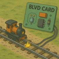
The Block Low Voltage Detection (BLVD) Card is a vital component for model railway enthusiasts using the LCC Fusion Project. This card continuously monitors the voltage levels of individual track blocks to ensure they remain within safe operating limits. It is designed to detect when the voltage drops below a predefined threshold, indicating potential issues such as poor connections, excessive load, or power supply problems.
Click  to listen to an audio explanation.
flowchart LR;
subgraph layout ["Train Layout"];
direction LR;
track["Track Block (4x)"];
bb[Block Breakout Board];
c["BLVD Card (16x)"];
nodeCard[Node Card];
can["CAN Network"]

track --> |"Voltage"|bb;
bb --> |"Low Voltage (yes/no)"|c;
c --> |"GPIO on/off"|nodeCard;
nodeCard--> |"Events (Low Voltage)"|can;
end;
classDef lSalmonStyle fill:#FFA07A,stroke:#333,stroke-width:2px,font-size:24px;
class c lSalmonStyle;
classDef lightGrayStyle fill:#d3d3d3,stroke:#333,stroke-width:2px,font-size:24px;
class layout lightGrayStyle;
Key Features:
- Voltage Monitoring: Continuously measures the voltage across track blocks.
- Low Voltage Indicators: When configured with the LCC Configuration Tool, LCC Events are generated when a block’s voltage drops below 12 VDC. In addition, an LED status indicator on the card turns on.
- Comparator Circuit: Utilizes an LM393 comparator to compare block voltage against a stable reference voltage.
- Visual Indicators: Supports LED indicators for each block, providing real-time status.
- MCP23017 Integration: Interfaces with MCP23017 GPIO expander to report low voltage conditions to a central controller.
- Protection: Includes TVS diode protection to safeguard against voltage spikes.
When to Use It:
- Track Power Monitoring: Essential for ensuring consistent power delivery to locomotives.
- Fault Detection: Quickly identifies and alerts to low voltage conditions that could affect train operation.
- Maintenance: Aids in diagnosing and troubleshooting electrical issues within the layout.
By integrating the BLVD Card into your LCC Fusion Project, you can enhance the reliability and performance of your model railway system, ensuring smooth and uninterrupted operation of your locomotives and other track components.
The BLVD Card hardware configuration includes:
- communication address; I2C bus (0 or 1) and address offset (0-7)
Common Causes of Low Voltage in Model Railway Layouts
- Short Circuits: Direct connections between VDC+ and GND, often due to derailments or wiring issues, can cause significant voltage drops.
- High Current Draw: Multiple locomotives or accessories drawing excessive current from the same track block can lower voltage levels.
- Poor Connections: Loose, corroded, or poorly soldered connections increase resistance, causing voltage drops.
- Long Wire Runs: Extended wiring increases resistance, leading to voltage loss over distance.
- Faulty Power Supply: A malfunctioning or underpowered supply can fail to maintain stable voltage levels.
- Dirty Tracks: Dust and dirt on the tracks can impede electrical contact, resulting in lower voltage at the rails.
System Overview
Here’s an explanation of the diagram below.
flowchart LR;
can["CAN Network"];
subgraph layout ["Train Layout"];
  direction LR;
    subgraph blvd ["BLVD Card (16x)"];
    direction LR;
    comparator["Voltage Comparator <br/> (LM393 IC)"];
    expander["GPIO Expander <br/> (mcp23017)"];
    end
  track["Track Block (4x)"] --> bb["Block Breakout Board"];
  bb --> |"Voltage <br/> (level)"| comparator;
  comparator --> |"GPIO Input <br/> (High/Low)"| expander
  expander -->|"GPIO Output<br/>(High/Low)"| n[Node Card];
  n -->|"LCC Event<br/>(Normal/Low)"| can;
end;
classDef lSalmonStyle fill:#FFA07A,stroke:#333,stroke-width:2px,font-size:24px;
class blvd lSalmonStyle;
classDef lightGrayStyle fill:#d3d3d3,stroke:#333,stroke-width:2px,font-size:24px;
class layout lightGrayStyle;
Assembly and Component Placement
This section combines both the component specifications and the assembly instructions to ensure a smooth assembly process. Below is a comprehensive list of components, their placement on the PCB, and orientation details to assist you during assembly.
High-Level Steps for Assembly:
- PCB for the card can be ordered from any PCB fabricator using these Gerber Files.
- Clean PCB with alcohol to remove residue. See Cleaning_PCB for details.
- See also: Soldering Tips
- PCB Components - listing of components used for PCB assembly
- PCB Parts - listing of parts used for PCB assembly
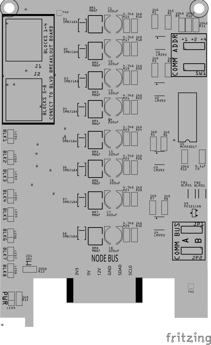
Below is a list of the PCB components used for this card (see diagram before reference):
![]()
![]()
| Component Identifier | Count | Type | Value | Package | Purpose | Orientation |
|---|---|---|---|---|---|---|
| Bridge Rectifiers | ||||||
| BR1-BR8 | 8 | Bridge Rectifier | MB6F | SOP-4 | Converts DCC pulsating AC-like waveform into a DC-like pulsating waveform for current detection. | Position IC’s indent to PCB right edge) |
| Capacitors | ||||||
| C1 - C8 | 8 | Capacitor-Polymer Solid | 100uF | 6.3x5.8mm SMD | Smooths DC signal. | Cathode is position to PCB’s top edge |
| C9 | 1 | Capacitor-Ceramic | 0.1uF | 1206 X7R | Conditions/filters the current for the IC (U1). | None |
| Diodes | ||||||
| D1-D8 | 8 | TVS Diode | SMBJ18A | SMB SMD | Protects from high-voltage transients (>29 VDC). | Cathode end has a white line and positioned towards PCB left edge |
| D9 | 1 | ESD Diode | PESD1CAN | SOT-23 SMD | Provides I2C data bus electrostatic discharge (ESD) protection. | None |
| ZD1 | 1 | Zener Diode | 18 VDC | 1206/DO-213 SMD | Creates a reference voltage determining lower track block voltage. | Cathode end has a white line and positioned towards PCB left edge |
| Filters & Noise Suppression | ||||||
| FB1, FB2 | 2 | Ferrite Bead | BLM31PG121SN1L | 1206 SMD | Suppresses noise on I2C data lines. | None |
| Connectors | ||||||
| J1, J2 | 2 | RJ45 Socket | 8P8C | PTH | Provides network cable (CAT5/6) connection to (1 or 2) Block Breakout Boards. | Fits only one way |
| Resistors | ||||||
| R1-R8 | 8 | Resistor | 1kΩ | 1206 SMD | Limits current to the MCP23017 GPIO pins and block low voltage LEDs. | None |
| R9, R10, R11 | 3 | Resistor | 10kΩ | 1206 SMD | Limits current to SW1 and MCP23017 for the I2C address. | None |
| R12 | 1 | Resistor | 10kΩ | 1206 SMD | Current limiting for MCP23017 reset. | None |
| R13 | 1 | Resistor | 200Ω | 1206 SMD | Current limiting for diode (reference voltage). | None |
| R14 | 1 | Resistor | 1kΩ | 1206 SMD | Current limiting for power LED. | None |
| R15, R17, R19, R21, R23, R25, R27, R29 | 8 | Resistor | 4.7kΩ | 1206 SMD | Voltage Divider to track is 3 VDC for comparator input | None |
| R16, R18, R20, R22, R24, R26, R28, R30 | 8 | Resistor | 1kΩ | 1206 SMD | Voltage Divider to track is 3 VDC for comparator input | None |
| Selectors & Indicators | ||||||
| JP1, JP2 | 2 | Male Header | 3P, 0.1” spacing | PTH | Used for COMM BUS selection (I2C hardware bus) for either BUS A or BUS B. | None |
| SH1, SH2 | 2 | Jumper Cap | 2.54mm | — | Used with I2C Bus and Vcc selections. Recommend tall caps for ease of use. | None |
| SW1 | 1 | DIP / Slide Switch | 3P, 2.54mm | PTH | Used for COMM ADDR selection (I2C address offset, 0-7). | Position ON towards PCB top edge |
| LED1 - LED8 | 8 | LED | Green | 1206 SMD | Used as block low voltage indicators, green when voltage is >12 VDC. | Reference back of LED, position cathode towards PCB bottom edge |
| LED9 | 1 | LED | Red | 1206 SMD | Power status indicator. | Reference back of LED, position cathode towards PCB bottom edge |
| ICs | ||||||
| U1-U4 | 4 | IC (Voltage Comparator) | LM393 or LM2903N | SO-8, SMD | Used for detecting low voltage (<12.1 VDC). | Small dot (pin 1) on package is positioned to PCB top/left edges |
| U5 | 1 | I/O Expander (MCP23017 IC) | SSOP28 | SMD | Controls 16 GPIO pins using I2C serial interface. | Dent on package positioned towards PCB bottom edge |
Tools Required
For a list of recommended tools, refer to List of recommended tools.
Testing and Verification
Configure the BOD Card:
-
Select the
COMM BUSby positioning (2) Jumper Caps on eitherAorBmale header pins (JP1, JP2) -
Select the
COMM ADDRESSswitch (SW1) by sliding each of the 3 switches to either theONorOFFposition. Setting a switch to ON increments the address by 1, 2, or 4 for an address range of 0 to 7. Up to 8 devices can then be configured forAand 8 forB.
The following test and verifications of the card should be performed after a through inspection of the card’s soldering. Check all of the PTH component pins and SMD pads. Make sure there are no solder bridges between pins and pads.
Visual Inspection
-
Initial Check: Examine the board for any obvious issues like missing components, solder bridges, or components that are misaligned or not fully seated.
-
Solder Joint Inspection: Use a magnifying glass or a microscope to inspect solder joints. Look for cold solder joints, insufficient or excessive solder, or any shorts between pads.
-
Component Orientation: the IC’s are correctly oriented according to the PCB silkscreen or schematic.
Connectivity Testing
Continuity Check: Use a multimeter in continuity mode to check for shorts between power rails and ground, and to ensure there are no open circuits in critical connections.
Power-Up Tests
- Assembly a tested Power Module to the LCC Fusion Node Card.
- Apply Power to the Power Module and verify the following:
- Check for Hot Components: Feel for components that are overheating, which could indicate a problem like a short circuit or incorrect component.
Functional Testing
Functional testing of the card can be performed after completing the power-up testing. Testing consists of testing network communiations, followed by the sensing of current in a layout track block.
HW Communications Testing
Communications testing verifies the LCC Node can communicate with the BOD Card’s I2C IC via the Node Bus Hub connections. This is performed using the LCC Fusion Node Card’s testing firmware and a serial monitor.
-
Insert the BOD Card into a Node Bus Hub along with a LCC Fusion Node Card.
-
Install LCC Fusion Project firmware that includes serial monitor for testing.
-
Verify that the I2C connection between the LCC Fusion Node Card and the BOD Card work.
See Testing I2C Cards for details on how to test the communications for a I2C enabled card.
MCP IC Testing
After hardware communication has been established, to verify the MCP IC, use the Node’s serial monitor to simulate an input from each of card’s input pins as follows:
- In the serial monitor’s input, enter
Mfor the LCC Node’s serial monitor Main Menu. - Select
[1] Node Managementand[1] Device Testing Management - Select
[5] Simlulate MCP Device Input - From the list of MCP devices, select the device # for the BOD Card being tested
- Enter the number for the pin to tested.
- Using the JMRI LccPro event monitoring tool, verify the correct Event ID was issued.
Track Block Testing
After validating the LCC Fusion Node Card can communicate (find) the BOD Card, test each of the BOD Card block connections.
Track block detection verification is performed using a Block Breakout Board connected to a track block.
-
Connect a network cable (CAT5/6) to one of the BOD Card’s RJ45 connector.
- Connect the other end of the network cable to (1) Block Breakout Board.
- Connect one of the Test Track rails directly to the Track Bus VDC+ connection.
- Connect the other Test Track rails to one of the Block Breakout Board block connections (BLK1 - BLK4)
- Connect the Test Track Bus GND to the Block Breakout Board TRACK BUS GND connection
- Configure each of the card’s device lines using an LCC CDI Configuration Tool.
- Open an LCC Event Monitoring tool (e.g. JMRI LccPro Event Monitoring tool).
-
Test each of the Breakout Board device connections using a locomotive (one at a time)
- draw current on the track by either
- placing a 10KΩ resistor across the track, or
- placing a locomotive on to the track
- Turn on the Track Power (let locomotive idle)
- Validate the configure Event ID for Block Occupied is sent by viewing the Event Monitoring tool
- draw current on the track by either
- Repeat testing for all (8) BOD Card connections as follows:
- Connect the Block Breakout Board to the first RJ45 socket (J1) for blocks 1-4.
- Reconnect to 2nd RJ46 socket (J2) for blocks 5-8.
Safety Precautions
- See Safety Precautions.
Provisioning the Card
- See Provisioning a Card.
Troubleshooting
- See I2C Trouble Shooting.
Appendences
PCB Specifications
![]()
| Characteristic | Value |
|---|---|
| Max Blocks Monitored | 8 |
| Maximum Number of Cards per LCC Fusion Node Cluster | 161 |
| Low Voltage Threshold | 12 VDC |
| Max Track Voltage (determined by LM393 IC) | 36 VDC |
- The LCC Fusion Node Cluster can support up to 16 cards, distributed across two I2C hardware buses, with a maximum of 8 cards per bus.
- Note: total includes all cards using the I2C address range of
0x20(MCP23017 IC).
- Note: total includes all cards using the I2C address range of
How It Works
The Block Low Voltage Detection (BLVD) Card continuously monitors each track block’s voltage and isolates the block via its relay when an undervoltage (indicative of a short or overload) occurs. Here’s an overview of its key stages:
-
DCC Rectification
- Track V+ and GND feed a KBL406 bridge rectifier, converting the bipolar DCC waveform into pulsed DC.
-
Smoothing
- A 100 µF capacitor across the rectifier output smooths the pulses into a stable DC level for comparison.
-
Reference Generation
-
To comply with the NMRA DCC specification (which requires track voltage to remain above 12 V RMS for reliable decoder operation), the comparator threshold is set to detect when the DCC voltage drops below 12 V RMS.
-
A Zener diode provides the reference. By default, an 18 V Zener is used, which—when paired with the divider network below—yields a trip point at ~12 V RMS. Adjust the divider if you need to fine‑tune exactly 12 V:
R_top = 4.7 kΩ R_bot = 1 kΩ Scale ≈ 1 k / (4.7 k + 1 k) ≈ 0.175- Zener input: 18 V → 3.15 V at comparator inverting input
- Track-sense divider: 12 V RMS (≈17 V peak) → 2.98 V at comparator non-inverting input
-
The Zener is biased from the 12 V rail through a 200 Ω resistor to ensure ~5 mA knee current, keeping the reference stable.
-
-
Comparator Action
- The LM393 compares the smoothed DC (non‑inverting input) against the Zener reference (inverting input).
- When the track voltage falls below the reference, the comparator’s open‑collector output pulls LOW, signaling a fault.
-
Logic Interface
- The LM393 output ties to an MCP23017 GPIO pin configured as an input with pull‑up to 3.3 V, preventing the line from floating.
- On a LOW output, the MCP23017 registers the fault and your ESP32 firmware generates the corresponding “Low Voltage” LCC event.
-
Visual & Surge Protection
- An optional LED (anode to 3.3 V, cathode through a 1 kΩ resistor to the comparator output) lights when the comparator output is LOW.
- A TVS diode across Track VDC+ and GND shields the circuit from voltage spikes and transients.
This coordinated operation ensures reliable, configurable undervoltage detection and clear isolation of overloaded track blocks, while providing both visual and networked alerts to enhance layout safety and maintenance.
PCB Protection
To ensure the reliable operation and longevity of your Block Occupancy Detection (BOD) card, several protection components have been integrated. These components safeguard the BOD Card from overcurrent, voltage spikes, and electrical noise. Below is a brief overview of each protection element and its role:
![]()
| Protected Component | Protection Component | Function | Specifications | Location |
|---|---|---|---|---|
| Entire Circuit | TVS Diode SMBJ18A | Protects from high-voltage transients by clamping voltage spikes, preventing them from reaching sensitive components. | Stand-off Voltage: 5V Clamping Voltage: 29 VDC |
Across the Vcc and GND lines of the track voltage |
| MCP23017 GPIO | 10k ohm Resistor | Further limits current between the optocoupler output and the MCP23017 GPIO pin. | Value: 10k ohms | Between the optocoupler output and MCP23017 input |
| MCP23017 | Decoupling Capacitor 0.1 µF | Filters out high-frequency noise and transient voltage spikes from the power supply, ensuring a stable voltage for the MCP23017. | Value: 0.1 µF | Across Vcc and GND near the MCP23017 |
| I2C Lines from LCC Fusion Node Bus Hub | Ferrite Bead BLM31PG121SN1L | Provides high-frequency noise suppression on the I2C lines. | Impedance: 120 Ω at 100 MHz | In series with the SDA and SCL lines of the I2C bus |
| I2C Lines from LCC Fusion Node Bus Hub | ESD Protection Diode PESD1CAN | Protects the I2C lines from electrostatic discharge and voltage spikes. | Reverse Stand-off Voltage (Vr): 24 VDC Clamping Voltage (Vc): 40 VDC |
Across the SDA and SCL lines from the card’s edge connector to GND, near the MCP23017. |
| LEDs | Current Limiting | Protects LEDs from current overload. | Value: 120 Ω | In series with LED |