BOD Card Assembly Guide
Table of contents
Table of contents
Introduction
See the How to Use Assembly Guides for detailed instructions.
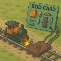
The Block Occupancy Detector Card (BOD Card), in synergy with the LCC Fusion Node Card, forms the detection backbone of the LCC Fusion Project system, facilitating precise detection of trains (locomotives and cars) within specified track blocks. This integration is pivotal for automating track occupancy detection, a core feature in advanced model railroad setups.
flowchart LR;
  can["CAN Network"];
  subgraph layout ["Train Layout"];
  direction LR;
  bb1[Block Breakout Board];
  bb2[Block Breakout Board];
  blocks1["Track Block (4x blocks)"];
  blocks2["Track Block (4x blocks)"]
  nodeCard[Node Card];

	blocks1 --> |"current"|bb1;
	blocks2 --> |"current"|bb2;
  c["BOD Card <br/> (8x blocks)"];
  bb1 --> |"Current <br/> (yes/no)"| c;
  bb2 --> |"Current <br/> (yes/no)"| c;
  c -->|"GPIO Output <br/> High/Low"| nodeCard;
  nodeCard -->|"LCC Event <br/> (occupied/unoccupied)"| can;
end;
classDef lSalmonStyle fill:#FFA07A,stroke:#333,stroke-width:2px,font-size:24px;
class c lSalmonStyle;
classDef lightGrayStyle fill:#d3d3d3,stroke:#333,stroke-width:2px,font-size:24px;
class layout lightGrayStyle;
Upon detecting a train within a block, the BOD Card generates an LCC event, signaling the occupancy status. This event is captured by the LCC Node, which, depending on the setup, could trigger various responses such as activating the PWM Card. This activation allows for nuanced control over railroad signals and other trackside functionalities, enhancing the realism and operational efficiency of the model railroad environment.
flowchart LR
  subgraph layout ["Train Layout"]
    direction LR;

    A["Train Approaches Block Entry<br> (Track A/B Power Active)"];
    B["1-Train Enters Isolated Block<br>(Rail B Gapped)<br>2-Current Flows Through Train<br>3-BOD Card Detects<br>Occupancy"];
    C["LCC Node Receives Detection<br>via MCP23017"];
    D["1-Train Exits Block<br>2-No Current Flow<br>3-BOD Clears Detection"];
    E["LCC Node Sends Block <br>Cleared Event"];

    A --> B --> C --> D --> E
  end

  classDef actionStyle fill:#bbf,stroke:#333,stroke-width:2px,font-style:italic,font-size:16px;
  class A,B,C,D,E actionStyle;
Detecting Positioning Turnout Points
The BOD Card can also be used to determine turnout points have been thrown or closed. This is performed by connecting one of the BOD Card’s block lines one of points along with a 10KΩ resistor. This will result in the BOD Card detecting a current when that point’s rail is moved and touches a side rail. The resulting ‘Occupied’ LCC event generated can be used to indicate the state of the point. This is useful for turnout motors that are not wired to a switch tied to the points.
Note: this is not required for TORTOISE™ and DCCconcepts Cobalt Omega Classic Point Motor (CB1A) switch machines, which have a builtin switch for detecting turnout point positioning.
The BOD Card hardware configuration includes:
- communication address; I2C bus (0 or 1) and address offset (0-7)
Assembly-Configuration Options
The BOD Card supports multiple assembly configurations to fit various use cases.
![]()
<img src="/LccFusionProject/assets/images/pcbs/Bod_Card/Bod_Card_Options_pcb.png" style="zoom:100%;" />
The PCB diagram shown above highlights different components based on their associated configuration. Each color-coded component corresponds to a specific configuration, which is further detailed in the table below.
To use this reference effectively:
- Match the Colors: Each assembly option in the table has a matching color in the PCB diagram. This helps identify which components are needed for a specific configuration.
- Locate Components Quickly: The highlighted component designators (e.g., D5, J1, JP2) on the PCB indicate where each part is placed.
- Identify Required vs. Optional Parts: The table differentiates between required components (essential for functionality) and optional components (enhancements or variations).
- Cross-Reference for Clarity: If you’re unsure about a part’s placement, use the designator labels on the PCB along with the descriptions in the table.
This approach ensures a clear, visual guide for assembling the Node Card based on your specific needs.
![]()
| Configuration | Required/Optional | Description | Required Components | Optional Components |
|---|---|---|---|---|
| Block Breakout Board Connection | Required | Network cable socket connectors to Block Breakout Board (or directly to blocks) | • Connectors: RJ45 socket J1, and/or J2 | None |
| Current Detection | Required | Detect current flowing through block connections | • I2C Port Expander: MCP23017 IC U1 , current limiting resistor R20, current smoothing capacitor C1 • Protection: fuses F1-F8, TVS Diodes D1-D8, current limiting resistors R1-R8, R12-R19 • Current Smoothing: capacitors C2-C9 • AC to DC Current Conversion: bridge rectifiers BR1-BR8 • Current Detection: Optocouplers U2-U9 |
• Detection Circuits: each set, for example for block 1; F1, D1, R1, R12, C2, BR1 |
| Communications Connection | Required | I2C Communications to Node Card | • Bus Selection: slide switch SW1, current limiting resistors R9, R10, R11 • Address Selection: 3-Pin Male Headers JP1, JP2 |
None |
| I2C BUS ESD Protection and Noise Filtering Support | Required | I2C Low Voltage Detection and Correction | • CAN Bus Noise Suppression: Ferrite beads FB1 and FB2 | • I2C Bus Protection: Diode D9 (for ESD protection on the I2Cdata bus) |
| Power and Block Detection Indicators Option | Optional | Setup for Power and Block Detection Indicators | • Block Detection Indicators LED Diode LED1 - LED8 • Power Indicator LED diode LED9, current limiting resistor R21 |
None |
Assembly and Component Placement
This section combines both the component specifications and the assembly instructions to ensure a smooth assembly process. Below is a comprehensive list of components, their placement on the PCB, and orientation details to assist you during assembly.
High-Level Steps for Assembly:
- PCB for the card can be ordered from any PCB fabricator using these Gerber Files.
- Clean PCB with alcohol to remove residue. See Cleaning_PCB for details.
- See also: Soldering Tips
- PCB Components - listing of components used for PCB assembly
- PCB Parts - listing of parts used for PCB assembly
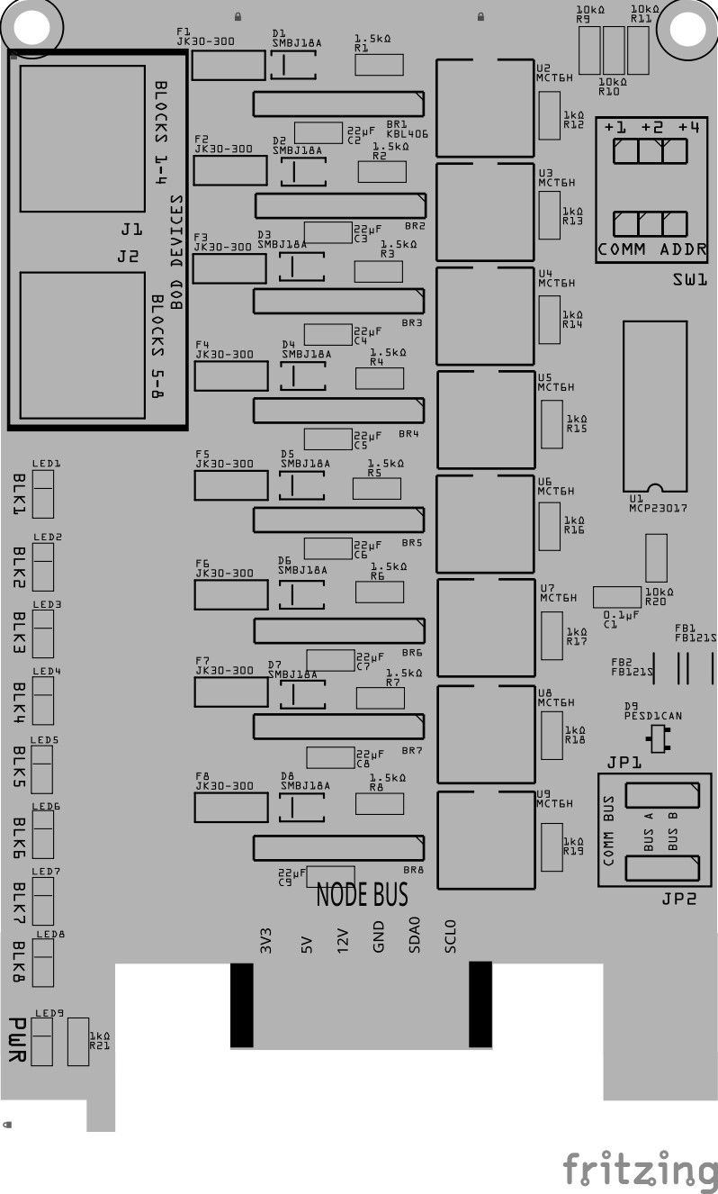
Below is a list of the PCB components used for this card (see diagram before reference):
![]()
![]()
| Component Identifier | Count1 | Type | Value | Package | Purpose | |
|---|---|---|---|---|---|---|
| Bridge Rectifiers | ||||||
| BR1-BR8 | 8 | Bridge Rectifier | KBL406, 4A | PTH | Converts the DCC pulsating AC-like waveform into a DC-like pulsating waveform for current detection without interfering with DCC signals. | Position the rectifier’s clipped corner (pin 1) toward PCB right edge |
| Capacitors | ||||||
| C1, C10 | 1 | Capacitor-Ceramic | 0.01uF | 1206 | Conditions/filters the current for IC (U1). | None |
| C2-C9 | 8 | Capacitor-Ceramic | 22uF | 1206 | Smooths incoming current for better detection when using resistor-equipped wheelsets. | None |
| Diodes | ||||||
| D1-D8 | 8 | TVS Diode | SMBJ18A | SMB | Protects from high-voltage transients (>29 VDC). | Cathode end has a white line and positioned towards PCB left edge |
| D9 | 1 | ESD Diode | PESD1CAN | SOT-23 SMD | I2C data bus electrostatic discharge (ESD) protection. | None |
| Filters & Noise Suppression | ||||||
| FB1, FB2 | 2 | Ferrite Bead | BLM31PG121SN1L | 1206 SMD | Noise suppression for I2C data lines. | None |
| F1-F8 | 8 | Fuse-PTC Polymer | JK30, 3A, 16 VDC (or more) | 5.1mm pitch, PTH | Protects from sustained overcurrent conditions. | None |
| Connectors | ||||||
| J1, J2 | 2 | RJ45 Socket | 8P8C | PTH | Network cable (CAT5/6) connection to 1 or 2 Block Breakout Board. | Fits only one way |
| Resistors | ||||||
| R1-R8 | 8 | Resistor | 1.5KΩ | 1206 SMD | Limits current from the track rail to the optocoupler. | None |
| R9-R10 | 3 | Resistor | 10KΩ | 1206 SMD | Limits current to SW1 and MCP23017 for I2C addressing. | None |
| R12-R19 | 8 | Resistor | 1KΩ | 1206 SMD | Limits current to status LEDs. | None |
| R20 | 1 | Resistor | 10KΩ | 1206 SMD | Limits current to the MCP23017 reset pin. | None |
| Selectors & Indicators | ||||||
| JP1, JP2 | 2 | Male Header | 3P, 0.1” spacing | PTH | Used for COMM BUS selection (I2C hardware bus) for either BUS A or BUS B. Must match LCC Node configuration (CDI). | None |
| SH1, SH2 | 2 | Jumper Cap | 2.54mm | N/A | Used with I2C Bus and Vcc selections. Recommend tall caps for ease of use. | None |
| SW1 | 1 | DIP / Slide Switch | 3P, 2.54mm | N/A | Used for COMM ADDR selection (I2C address offset, 0-7). | Position ON towards PCB top edge |
| LED1-LED8 | 8 | LED | Red | 1206 SMD | Indicates block occupancy (current flow). | Reference back of LED, position cathode towards PCB top edge |
| LED9 | 1 | LED | Green | 1206 SMD | PWR status indicator. | Reference back of LED, position cathode towards PCB top edge |
| ICs | ||||||
| U1 | 1 | IC | MCP23017 | SSOP28 SMD | I/O Expander using I2C serial interface to control 16 GPIO pins. | Position IC’s indent (pin 1) towards PCB bottom edge |
| U2-U9 | 8 | Optocoupler | MCT6H | DIP-8 PTH | Detects current flow. | Position IC’s indent (pin 1) towards PCB top edge |
| U10 | 1 | EEPROM | AT24C02 | SOIC-8 | Memory for card’s type and description | IC indent is positioned towards PCB right edge |
- For components with counts of 8, only one of the specified component is required for a specific DOD detection circuits.
Tools Required
For a list of recommended tools, refer to List of recommended tools.
Safety Precautions
- See Safety Precautions.
Testing and Verification
Configure the BOD Card:
-
Select the
COMM BUSby positioning (2) Jumper Caps on eitherAorBmale header pins (JP1, JP2) -
Select the
COMM ADDRESSswitch (SW1) by sliding each of the 3 switches to either theONorOFFposition. Setting a switch to ON increments the address by 1, 2, or 4 for an address range of 0 to 7. Up to 8 devices can then be configured forAand 8 forB.
The following test and verifications of the card should be performed after a through inspection of the card’s soldering. Check all of the PTH component pins and SMD pads. Make sure there are no solder bridges between pins and pads.
Visual Inspection
-
Initial Check: Examine the board for any obvious issues like missing components, solder bridges, or components that are misaligned or not fully seated.
-
Solder Joint Inspection: Use a magnifying glass or a microscope to inspect solder joints. Look for cold solder joints, insufficient or excessive solder, or any shorts between pads.
-
Component Orientation: the IC’s are correctly oriented according to the PCB silkscreen or schematic.
Connectivity Testing
![]()
Power-Up Tests
- Assembly a tested to the LCC Fusion Node Card.
- Apply Power to the Power Module and verify the following:
- Check for Hot Components: Feel for components that are overheating, which could indicate a problem like a short circuit or incorrect component.
Functional Testing
Functional testing of the card can be performed after completing the power-up testing. Testing consists of testing network communiations, followed by the sensing of current in a layout track block.
HW Communications Testing
Communications testing verifies the LCC Node can communicate with the BOD Card’s I2C IC via the Node Bus Hub connections. This is performed using the LCC Fusion Node Card’s testing firmware and a serial monitor.
-
Insert the BOD Card into a Node Bus Hub along with a LCC Fusion Node Card.
-
Install LCC Fusion Project firmware that includes serial monitor for testing.
-
Verify that the I2C connection between the LCC Fusion Node Card and the BOD Card work.
See Testing I2C Cards for details on how to test the communications for a I2C enabled card.
MCP IC Testing
After hardware communication has been established, to verify the MCP IC, use the Node’s serial monitor to simulate an input from each of card’s input pins as follows:
- In the serial monitor’s input, enter
Mfor the LCC Node’s serial monitor Main Menu. - Select
[1] Node Managementand[1] Device Testing Management - Select
[5] Simlulate MCP Device Input - From the list of MCP devices, select the device # for the BOD Card being tested
- Enter the number for the pin to tested.
- Using the JMRI LccPro event monitoring tool, verify the correct Event ID was issued.
Track Block Testing
After validating the LCC Fusion Node Card can communicate (find) the BOD Card, test each of the BOD Card block connections.
Track block detection verification is performed using a Block Breakout Board connected to a track block.
- Connect a network cable (CAT5/6) to one of the BOD Card’s RJ45 connector.
- Connect the other end of the network cable to (1) Block Breakout Board.
- Connect one of the Test Track rails directly to the Track Bus VDC+ connection.
- Connect the other Test Track rails to one of the Block Breakout Board block connections (BLK1 - BLK4)
- Connect the Test Track Bus GND to the Block Breakout Board TRACK BUS GND connection
- Configure each of the card’s device lines using an LCC CDI Configuration Tool
- Open an LCC Event Monitoring tool (e.g. JMRI Event Monitoring tool).
-
Test each of the Breakout Board device connections using a locomotive (one at a time)
- draw current on the track by either
- placing a 10KΩ resistor across the track, or
- placing a locomotive on to the track
- Turn on the Track Power (let locomotive idle)
- Validate the configure Event ID for Block Occupied is sent by viewing the Event Monitoring tool
- draw current on the track by either
- Repeat testing for all (8) BOD Card connections as follows:
- Connect the Block Breakout Board to the first RJ45 socket (J1) for blocks 1-4.
- Reconnect to 2nd RJ46 socket (J2) for blocks 5-8.
Provisioning the Card
- See Provisioning a Card.
Troubleshooting
- See I2C Trouble Shooting.
Appendences
PCB Specifications
Specifications for the card include:
![]()
| Characteristic | Value |
|---|---|
| Maximum BOD Detections | 8 |
| Maximum Block Breakout Board | 2 |
| Maximum Cards per LCC Fusion Node Cluster | 161 |
| Maximum Track Current | 3.5A2 |
| Minimum Track Voltage | 14.2 VDC3 |
| Max Track Voltage (determined by MCT6H IC) | 30 VDC |
- The LCC Fusion Node Cluster supports up to 16 cards, distributed across two I2C hardware buses, with a maximum of 8 cards per bus.
- Note: This total includes all cards using the I2C address range of
0x20(MCP23017 IC).
- Note: This total includes all cards using the I2C address range of
- The BOD Card uses 32mil PCB traces, to support up to 3.5A. The card also uses a 3.5A fuse, and a 6A bridge rectifier.
- The minimum track voltage is 14.2 VDC due to the voltage drop from the bridge rectifier on the BOD Card (which reduces voltage by 2.2 VDC). DCC decoders require at least 12 VDC, in accordance with NMRA DCC standards.
How It Works
The following outlines the flow of activity for the BOD Card:
The firmware of the LCC Fusion Node Card interfaces with the BOD Card’s port expander (MCP23017), leveraging the bus and address details specified in the card’s CDI I2C section.
The BOD Card’s block occupancy detection details are as follows:
-
One of the layout track rails—typically Rail B—is isolated into ‘blocks’ by placing insulated rail joiners at both ends. These blocks are used to detect the presence of a train within a designated section of track. Common block placements include approach sections before a turnout, the turnout itself, and each of the diverging and main routes beyond.
-
When a locomotive (cab) or a car equipped with a resistor between its wheelset hubs enters an isolated block, current flows between the two rails within that block. The DCC current path includes both Rail A and Rail B through the train.
Car detection can be performed using a 10kΩ resistor wired between one of the wheelset hubs. Refer to Wiring Wheelsets for Enhanced Block Occupancy Detection.
-
To monitor this current, the Rail B side of each block must be routed through the BOD Card, which is connected in series with the block’s Rail B. This is done using a Block Breakout Board, which provides four connectors labeled:
- 1–4 TRACK BLOCKS GAPPED RAIL B – These accept the Rail B “drop wires” from each isolated block.
- TRACK BUS B – This single connector returns all monitored blocks to the main DCC layout Rail B bus.
Wheelset detection can be erratic because of poor contact with track rails. To help improve detection reliability, a 22 µF ceramic capacitor is used to smooth brief interruptions in current flow.
-
Optional Feature: Block Rail A Power Control (Stop Block Support)
To support train presence detection even when Rail A is turned off, the Block Breakout Board now includes an optional Block Detection Compatibility with Power Cut, ensuring detection is preserved while power is removed from the block to stop a train. When enabled:
- A 10kΩ resistor in series with a SS310 Schottky diode connects Track Bus A to each isolated block’s Rail B.
- This allows a small “leakage” current to flow through the train (assuming it includes resistor-equipped wheelsets), even when Rail A is intentionally powered down (e.g., for stop blocks or signaling).
- The diode ensures current flows into the block only, preventing unwanted backfeed between blocks or into the Track Bus.
Each block’s trickle path is isolated and user-selectable via a jumper on the breakout board.
NoNote: Both block rails A and B must be gapped to fully isolate the block. Rail A is controlled via a Output Card connected to a Relay Breakout Board; Rail B must be routed through the BOD Card for occupancy detection.
-
The DCC current path flows as follows:
-
From the Track Block Rail A — or, if Rail A is disabled, from the Track Bus A via the optional 10kΩ + diode trickle path — current flows into the block,
-
Through the train’s motor or resistor
-
Out via Rail B, which is connected to the BOD Card through the Block Breakout Board
-
Then through the BOD Card’s sensing components
-
And finally back to the main DCC Rail B bus via the Track Bus B return wire
-
-
As this current passes through the BOD Card:
-
An inline resettable 3A fuse protects the circuit from overcurrent conditions, disconnecting the block temporarily during faults and automatically restoring operation afterward.
-
A transient voltage suppression (TVS) diode (SMBJ18A) across the input clamps voltage spikes that could occur on the DCC line, protecting the sensing circuitry.
-
A 22 µF electrolytic capacitor filters out ripple and high-frequency noise from the DCC signal.
-
A bridge rectifier (e.g., KBL400) routes the AC-like DCC signal through the appropriate pair of pins to forward-bias the internal LEDs of an optocoupler. Pins 1 and 4 of the rectifier are typically tied to support symmetrical current sensing.
-
A 1.5kΩ resistor limits the current flowing into the optocoupler’s internal LEDs.
-
-
As the current flows through the rectifier and optocoupler:
-
The optocoupler turns ON, pulling the corresponding MCP23017 GPIO input LOW.
-
When no current flows, the optocoupler’s output remains HIGH, pulled up by a 10kΩ resistor.
-
The optocoupler contains two LEDs wired in opposite directions, allowing it to detect DCC current in either polarity. This means that regardless of which rail is currently “positive,” one LED is always forward-biased, enabling detection of current flow throughout both halves of the DCC waveform.
-
-
When current is detected, the MCP23017 pin (A0–A7) goes LOW, and the LCC Node firmware reads this state change and issues an appropriate LCC Event to the layout network.
-
Status LEDs on the BOD Card illuminate when the optocoupler output is LOW (i.e., current is detected). Each LED’s anode is tied to 3.3V, and its cathode is connected to the optocoupler’s output through a 1kΩ current-limiting resistor.
Connections
The purpose of the BOD Card is to provide detection of track block occupancy by detecting current.
![]()
| Component Designator | Connector Label | Connector Type | Connection Number | Description | | ——————– | ——————– | ————– | ——————— | ———————————————————— | | J1, J2 | BOD DEVICES | RJ45 Socket | 1/2, 3/4, 5/6, 7/8 | Use 1 or 2 network cables to connect to the **Block Breakout Board ** which connects to the track blocks. |
PCB Protection
To ensure the reliable operation and longevity of your BOD Card, several protection components have been integrated. These components safeguard the BOD Card from overcurrent, voltage spikes, and electrical noise. Below is a brief overview of each protection element and its role:
![]()
| Protected Component | Protection Component | Function | Specifications | Location |
|---|---|---|---|---|
| Entire Circuit | Optocoupler | Provides electrical isolation, protecting the circuit from high voltages and noise by isolating different sections. | Current Rating: 60 mA Surge Current: 1.5 A |
Between the track voltage input and the MCP23017 GPIO pin |
| Entire Circuit | PPTC Polyfuse | Protects from sustained overcurrent conditions by increasing resistance when the current exceeds 3A. Resets once the fault condition is cleared. | Hold Current: 3A Trip Current: 6A |
In series with the track Vcc line. Adjust the fuse type to match the MAX amperage expected within the block. |
| Entire Circuit | TVS Diode SMBJ18A | Protects from high-voltage transients by clamping voltage spikes, preventing them from reaching sensitive components. | Stand-off Voltage: 18 VDC Clamping Voltage: 29.2 VDC |
Across the Vcc and GND lines of the track voltage |
| LEDs | 1K ohm Resistor | Limits current to LED to create about 15% brightness | Value: 1k ohms | Between the optocoupler output and LED anode |
| Optocoupler | 1.5K ohm Resistor | Limits inrush current to the optocoupler, protecting it from sudden surges. | Value: 1.5k ohms | In series with the anode of the optocoupler |
| MCP23017 GPIO | 10k ohm Resistor | Further limits current between the optocoupler output and the MCP23017 GPIO pin. | Value: 10k ohms | Between the optocoupler output and MCP23017 input |
| MCP23017 | Decoupling Capacitor 0.1 µF | Filters out high-frequency noise and transient voltage spikes from the power supply, ensuring a stable voltage for the MCP23017. | Value: 0.1 µF | Across Vcc and GND near the MCP23017 |
| I2C Lines from LCC Fusion Node Bus Hub | Ferrite Bead BLM31PG121SN1L | Provides high-frequency noise suppression on the I2C lines. | Impedance: 120 ohms at 100 MHz | In series with the SDA and SCL lines of the I2C bus |
| I2C Lines from LCC Fusion Node Bus Hub | ESD Protection Diode PESD1CAN | Protects the I2C lines from electrostatic discharge and voltage spikes. | Reverse Stand-off Voltage (Vr): 24 VDC Clamping Voltage (Vc): 40 VDC |
Across the SDA and SCL lines from the card’s edge connector to GND, near the MCP23017. |
Summary
These protection components work together to safeguard the BOD Card from various electrical faults. The polyfuse provides overcurrent protection, the TVS diode clamps high-voltage spikes, the current limiting resistors control the current flow, and the decoupling capacitor filters out noise. The ferrite bead suppresses high-frequency noise on the I2C lines, and the ESD protection diode protects the I2C lines from electrostatic discharge and voltage spikes. The optocoupler provides electrical isolation, protecting the entire circuit from high voltages and noise. Together, they ensure the BOD Card operates reliably in a potentially harsh electrical environment.
References
- I2C GPIO Mapping (BOD Card)
The BOD Card receives occupancy detection signals from its breakout board. Each signal reflects whether current is flowing through the track block. Detected by a voltage drop across a diode and converted to TTL by an LM393 comparator.
| RJ45 Line | MCP23017 Pin | GPIO Line | Direction | Pull-up | Logic Levels | Purpose | Notes |
|---|---|---|---|---|---|---|---|
| L1 | GPA0 | GP0 | Input | Enabled | LOW = Occupied | Block 1 Detection | LM393 output from diode drop comparator |
| L2 | GPA1 | GP1 | Input | Enabled | LOW = Occupied | Block 2 Detection | LM393 output from diode drop comparator |
| L3 | GPA2 | GP2 | Input | Enabled | LOW = Occupied | Block 3 Detection | LM393 output from diode drop comparator |
| L4 | GPA3 | GP3 | Input | Enabled | LOW = Occupied | Block 4 Detection | LM393 output from diode drop comparator |
| L5 | GPA4 | GP4 | Input | Enabled | LOW = Occupied | Block 5 Detection | LM393 output from diode drop comparator |
| L6 | GPA5 | GP5 | Input | Enabled | LOW = Occupied | Block 6 Detection | LM393 output from diode drop comparator |
| L7 | GPA6 | GP6 | Input | Enabled | LOW = Occupied | Block 7 Detection | LM393 output from diode drop comparator |
| L8 | GPA7 | GP7 | Input | Enabled | LOW = Occupied | Block 8 Detection | LM393 output from diode drop comparator |