BRD Card Assembly Guide
Table of contents
Table of contents
Introduction
See the How to Use Assembly Guides for detailed instructions.

The Block Reversing Detection (BRD) Card is an essential component for model railway enthusiasts using the LCC Fusion Project. This card monitors the voltage across an turnout’s frog, isolated loop, or reversing track block and detects when a short circuit occurs — typically caused by a polarity mismatch as a train enters or exits the block. Upon detection, the BRD Card triggers a polarity reversal using an onboard latching relay, allowing seamless train operation through reverse loops, wyes, balloon tracks, or other reversing configurations. This automated detection and correction process enhances reliability and prevents layout shutdowns caused by electrical conflicts.
flowchart LR;
  subgraph layout ["Train Layout"];
  direction LR;
  frog["Turnout Frog"];
  loop1["Loop Track Block (2x)"]
  main1["Mainline Track Block (2x)"]
  turnout["Mainline Track Block (2x)"]
  bb1["BRD Breakout Board"];
    bb2["BRD Breakout Board"];
  c["BRD Card (16x)"];
  nodeCard["Node Card"];
  can["CAN Network"];

  loop1 --> |"voltage (short)"|bb1;
  bb1 -->|"current (reversal)"|loop1;
  main1 --> |"current"|bb1;
  bb1 -->|"reversal (yes/no"|c;

  frog --> |"voltage (short)"|bb2;
  bb2 -->|"current (reversal)"|frog;
  turnout --> |"current"|bb2;
  bb2 -->|"reversal (yes/no"|c;
  c -->|"GPIO Output <br/> High/Low"| nodeCard;
  nodeCard -->|"LCC Event <br/> (occupied/unoccupied)"| can;
end;
classDef lSalmonStyle fill:#FFA07A,stroke:#333,stroke-width:2px,font-size:24px;
class brdcard lSalmonStyle;
classDef lightGrayStyle fill:#d3d3d3,stroke:#333,stroke-width:2px,font-size:24px;
class layout lightGrayStyle;
flowchart LR;
subgraph layout ["Train Layout"];
	direction LR;
  A["Train Approaches Loop Entry<br> (Mainline - Track A/B)"];
  B["1 - Train Enters Loop Block<br>(Bridges Entry Gap)<br>2 - Short Detected by BRD<br/>3 - Toggle Relay<br/>4 - Match Mainline Polarity"];
  C["Train Inside Loop<br>(Polarity Now Correct)"];
  D["1 - Train Exits Loop<br>(Bridges Exit Gap)<br>2 - Short Detected by BRD<br/>3 - Toggle Relay<br>4 - Match Mainline Polarity"];
  E["Train Back on Mainline<br> (Now Opposite Direction)"];

  A --> B --> C --> D --> E
end;

classDef actionStyle fill:#bbf,stroke:#333,stroke-width:2px,font-style:italic,font-size:16px;
class A,B,C,D,E actionStyle;
Key Features:
- Polarity Conflict Detection: Continuously monitors the voltage across an isolated reversing block to detect shorts caused by polarity mismatches.
- Automatic Polarity Reversal: When a short is detected, the card triggers a latching relay to reverse the block’s polarity, resolving the fault automatically.
- Comparator Circuit: Utilizes an LM393 comparator to detect voltage drops relative to a 12V zener reference, identifying polarity-related short circuits.
- MCP23017 Integration: Interfaces with an MCP23017 GPIO expander to report the short detection status to a Node Card for event generation and monitoring.
- LCC Event Support: When configured with the LCC Configuration Tool, LCC Events are generated to report polarity reversals or short conditions across the CAN network.
- Visual Indicators: Optional onboard LEDs can display real-time status of polarity reversal or detection activity.
- Protection: Includes TVS diode protection and supports optional slow-blow or polyfuse-based current protection to guard against persistent or true shorts.
When to Use It:
Reverse Loops: Automatically corrects polarity mismatches as trains enter or exit reverse loops, preventing short circuits and layout shutdowns.
Wyes and Balloon Tracks: Handles polarity reversal in complex track geometries where train direction changes create electrical conflicts.
Crossover and Return Tracks: Useful in areas where blocks connect to differently polarized track sections, ensuring smooth transitions.
Turntable Approaches: Can be adapted to detect and correct polarity when locomotives reverse direction on turntable exits.
Automation and Reliability: Ideal for layouts requiring automated short detection and correction to support hands-free, uninterrupted operation.
The BLVD Card hardware configuration includes:
- communication address; I2C bus (0 or 1) and address offset (0-7)
System Overview
Here’s an explanation of the diagram below.
flowchart LR;
subgraph layout ["Train Layout"];
  direction LR;
    subgraph brd[" "];
    brdTitle["BRD Card<br>(Block Reversing Detection)"];
    direction LR;
    comparator["Short Detection Comparator <br/> (LM393 IC)"];
    expander["GPIO Expander <br/> (MCP23017)"];
    relay["Latching Relay <br/> (TQ2-L2-12V)"];
    end
  bb["BRD Breakout Board"];
  loop["Loop Track Rails A/B"]
  main["Main Track Rails A/B"]

  main --> |"voltage"|bb;
  loop <--> |"polarity"|bb;
  bb --> |"Rectified Voltage"| comparator;
  can["LCC CAN Network"]
  comparator --> |"Short Detected <br/> (Low Signal)"| expander;
  comparator --> |"Pulse to Relay Coil"| relay;
  relay --> |"polarity"|bb;
  expander -->|"GPIO Output<br/>(High/Low)"| n[Node Card];
  n -->|"LCC Event<br/>(Polarity Reversed)"| can;
end;
classDef lSalmonStyle fill:#FFA07A,stroke:#333,stroke-width:2px,font-size:24px;
class brd lSalmonStyle;
classDef lightGrayStyle fill:#d3d3d3,stroke:#333,stroke-width:2px,font-size:24px;
class layout lightGrayStyle;
Assembly and Component Placement
![]()
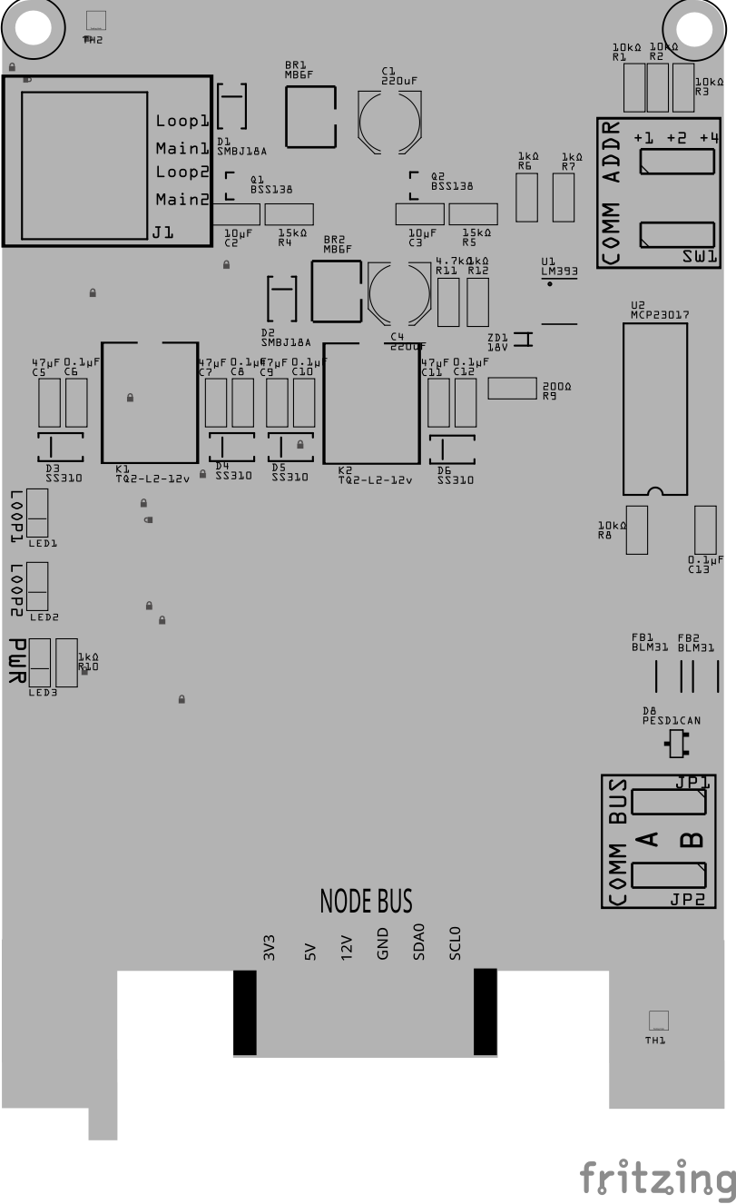
This section combines both the component specifications and the assembly instructions to ensure a smooth assembly process. Below is a comprehensive list of components, their placement on the PCB, and orientation details to assist you during assembly.
High-Level Steps for Assembly:
- PCB for the card can be ordered from any PCB fabricator using these Gerber Files.
- Clean PCB with alcohol to remove residue. See Cleaning_PCB for details.
- See also: Soldering Tips
- PCB Components - listing of components used for PCB assembly
- PCB Parts - listing of parts used for PCB assembly
Below is a list of the PCB components used for this card (see diagram before reference):
![]()
| Component Identifier | Count | Type | Value | Package | Purpose | Orientation |
|---|---|---|---|---|---|---|
| Bridge Rectifiers | ||||||
| BR1 | 2 | Bridge Rectifier | MB6F | SOP-4 | Converts DCC pulsating AC-like waveform into a DC-like pulsating waveform for current detection. | Position IC’s indent to PCB right edge) |
| Capacitors | ||||||
| C1, C4 | 2 | Capacitor-Polymer Solid | 100uF | 6.3x5.8mm SMD | Smooths DC signal. | Position Cathode to PCB bottom edge |
| C2, C3 | 2 | Capacitor-Ceramic | 0.1uF | 1206 | smooths pulse for the 150ms RC | None |
| C5, C7, C9, C11 | 4 | Capacitor-Ceramic | 47uF | 1206 | Bulk cap for smoothing current/voltage changes from relay coil | None |
| C6, C8, C10, C12 | 4 | Capacitor-Ceramic | 0.1uF | 1206 | Catch voltage spikes from relay coil | None |
| C13 | 1 | Capacitor-Ceramic | 0.1uF | 1206 | Conditions/filters the current for the MCP23017 IC. | None |
| C14 | 1 | Capacitor-Ceramic | 0.1uF | 1206 SMD | Decoupling Capacitor for IC Protection | None |
| Diodes | ||||||
| D1, D2 | 2 | TVS Diode | SMBJ18A | SMB SMD | Protects from high-voltage transients (>29 VDC). | Cathode end has a white line and positioned towards PCB left side |
| D3, D4, D5, D6 | 4 | Diode | SS310 | 1206 SMD | Clamps inductive kick-back from relay coils de-energizing | Position Cathode end has a white line and positioned towards PCB top side |
| D7 | 1 | ESD Diode | PESD1CAN | SOT-23 SMD | Provides I2C data bus electrostatic discharge (ESD) protection. | Fits only one way |
| ZD1 | 1 | Zener Diode | 16 VDC or 18 VDC | 1206/DO-213 SMD | Creates a reference voltage determining lower track block voltage. | Cathode end has a white line and positioned towards PCB bottom edge |
| Filters & Noise Suppression | ||||||
| FB1, FB2 | 2 | Ferrite Bead | BLM31PG121SN1L | 1206 SMD | Suppresses noise on I2C data lines. | None |
| Connectors | ||||||
| J1 | 1 | RJ45 Socket | 8P8C | PTH | Provides network cable (CAT5/6) connection BRD Breakout Board | Fits only one way |
| Resistors | ||||||
| R1, R2, R3 | 3 | Resistor | 10kΩ | 1206 SMD | Limits current to SW1 and MCP23017 for the I2C address. | None |
| R4, R5 | 2 | Resistor | 15kΩ | 1206 SMD | Debounces & pulse-stretches for the 150ms RC circuit | None |
| R6, R7 | 2 | Resistor | 1kΩ | 1206 SMD | Limits current to the MCP23017 GPIO pins and block low voltage LEDs. | None |
| R8 | 1 | Resistor | 10kΩ | 1206 SMD | Current limiting for MCP23017 reset. | None |
| R9 | 1 | Resistor | 200Ω | 1206 SMD | Current limiting for diode (reference voltage). | None |
| R10 | 1 | Resistor | 1kΩ | 1206 SMD | Current limiting for power LED. | None |
| R11 | 1 | Resistor | 4.7kΩ | 1206 SMD | Voltage Divider to track is 3 VDC for comparator input | None |
| R12 | 1 | Resistor | 1kΩ | 1206 SMD | Voltage Divider to track is 3 VDC for comparator input | None |
| Selectors & Indicators | ||||||
| JP1, JP2 | 2 | Male Header | 3P, 0.1” spacing | PTH | Used for COMM BUS selection (I2C hardware bus) for either BUS A or BUS B. | None |
| SH1, SH2 | 2 | Jumper Cap | 2.54mm | — | Used with I2C Bus and Vcc selections. Recommend tall caps for ease of use. | None |
| SW1 | 1 | DIP / Slide Switch | 3P, 2.54mm | PTH | Used for COMM ADDR selection (I2C address offset, 0-7). | Position ON towards PCB top. |
| LED1, LED2 | 2 | LED | Green | 1206 SMD | Used as block low voltage indicators, green when voltage is >12 VDC. | Reference back of LED, position cathode towards PCB bottom |
| LED3 | 1 | LED | Red | 1206 SMD | Power status indicator. | Reference back of LED, position cathode towards PCB bottom |
| ICs | ||||||
| U1 | 1 | IC (Voltage Comparator) | LM393 or LM2903N | SO-8, SMD | Used for detecting low voltage (<12.1 VDC). | Position IC’s dent towards PCB top/left edges |
| U5 | 1 | I/O Expander (MCP23017 IC) | SSOP28 | SMD | Controls 16 GPIO pins using I2C serial interface. | Position IC’s dent towards PCB bottom edge |
| U6 | 1 | EEPROM | AT24C02 | SOIC-8 | Memory for card’s type and description | IC indent is positioned towards PCB bottom edge |
| Transistors | ||||||
| Q1, Q2 | 2 | NPN Transistor | BSS138 | SOT-23 | Required | Controls CAN connections to terminator |
Tools Required
For a list of recommended tools, refer to List of recommended tools.
Testing and Verification
Configure the BOD Card:
-
Select the
COMM BUSby positioning (2) Jumper Caps on eitherAorBmale header pins (JP1, JP2) -
Select the
COMM ADDRESSswitch (SW1) by sliding each of the 3 switches to either theONorOFFposition. Setting a switch to ON increments the address by 1, 2, or 4 for an address range of 0 to 7. Up to 8 devices can then be configured forAand 8 forB.
The following test and verifications of the card should be performed after a through inspection of the card’s soldering. Check all of the PTH component pins and SMD pads. Make sure there are no solder bridges between pins and pads.
Visual Inspection
-
Initial Check: Examine the board for any obvious issues like missing components, solder bridges, or components that are misaligned or not fully seated.
-
Solder Joint Inspection: Use a magnifying glass or a microscope to inspect solder joints. Look for cold solder joints, insufficient or excessive solder, or any shorts between pads.
-
Component Orientation: the IC’s are correctly oriented according to the PCB silkscreen or schematic.
Connectivity Testing
Continuity Check: Use a multimeter in continuity mode to check for shorts between power rails and ground, and to ensure there are no open circuits in critical connections.
Power-Up Tests
- Assembly a tested Power Module to the LCC Fusion Node Card.
- Apply Power to the Power Module and verify the following:
- Check for Hot Components: Feel for components that are overheating, which could indicate a problem like a short circuit or incorrect component.
Functional Testing
Functional testing of the card can be performed after completing the power-up testing. Testing consists of testing network communiations, followed by the sensing of current in a layout track block.
HW Communications Testing
Communications testing verifies the LCC Node can communicate with the BOD Card’s I2C IC via the Node Bus Hub connections. This is performed using the LCC Fusion Node Card’s testing firmware and a serial monitor.
-
Insert the BOD Card into a Node Bus Hub along with a LCC Fusion Node Card.
-
Install LCC Fusion Project firmware that includes serial monitor for testing.
-
Verify that the I2C connection between the LCC Fusion Node Card and the BOD Card work.
See Testing I2C Cards for details on how to test the communications for a I2C enabled card.
MCP IC Testing
After hardware communication has been established, to verify the MCP IC, use the Node’s serial monitor to simulate an input from each of card’s input pins as follows:
- In the serial monitor’s input, enter
Mfor the LCC Node’s serial monitor Main Menu. - Select
[1] Node Managementand[1] Device Testing Management - Select
[5] Simlulate MCP Device Input - From the list of MCP devices, select the device # for the BOD Card being tested
- Enter the number for the pin to tested.
- Using the JMRI LccPro event monitor, verify the correct Event ID was issued.
Track Block Testing
After validating the LCC Fusion Node Card can communicate (find) the BOD Card, test each of the BOD Card block connections.
Track block detection verification is performed using a Block Breakout Board connected to a track block.
-
Connect a network cable (CAT5/6) to one of the BOD Card’s RJ45 connector.
- Connect the other end of the network cable to (1) Block Breakout Board.
- Connect one of the Test Track rails directly to the Track Bus VDC+ connection.
- Connect the other Test Track rails to one of the Block Breakout Board block connections (BLK1 - BLK4)
- Connect the Test Track Bus GND to the Block Breakout Board TRACK BUS GND connection
- Configure each of the card’s device lines using an LCC CDI Configuration Tool.
- Open an LCC Event Monitoring tool (e.g. JMRI Event Monitoring tool).
-
Test each of the Breakout Board device connections using a locomotive (one at a time)
- draw current on the track by either
- placing a 10KΩ resistor across the track, or
- placing a locomotive on to the track
- Turn on the Track Power (let locomotive idle)
- Validate the configure Event ID for Block Occupied is sent by viewing the Event Monitoring tool
- draw current on the track by either
- Repeat testing for all (8) BOD Card connections as follows:
- Connect the Block Breakout Board to the first RJ45 socket (J1) for blocks 1-4.
- Reconnect to 2nd RJ46 socket (J2) for blocks 5-8.
Provisioning the Card
- See Provisioning a Card.
Troubleshooting
- See I2C Trouble Shooting.
Safety Precautions
- See Safety Precautions.
Provisioning the Card
- See Provisioning a Card.
Troubleshooting
- See I2C Trouble Shooting.
Appendences
PCB Specifications
![]()
| Characteristic | Value |
|---|---|
| Max Loop Blocks Monitored | 1 |
| Maximum Number of Cards per LCC Fusion Node Cluster | 161 |
| Reverse Detection Threshold | 12 VDC |
| Max Track Voltage (determined by LM393 IC) | 36 VDC |
- The LCC Fusion Node Cluster can support up to 16 cards, distributed across two I2C hardware buses, with a maximum of 8 cards per bus.
- Note: total includes all cards using the I2C address range of
0x20(MCP23017 IC).
- Note: total includes all cards using the I2C address range of
How It Works
-
The Block Reversing Detection (BRD) Card monitors voltage drops caused by polarity conflicts in reversing track blocks and automatically flips track polarity via a latching relay. Here’s how it operates:
-
DCC Rectification
- Track V+ and GND from the isolated reversing block feed an MB6F bridge rectifier, converting the bipolar DCC waveform into pulsed DC for sensing.
-
Smoothing
- A 100 µF capacitor across the bridge output smooths the pulses into a stable DC level.
-
Reference Generation (Inverting Input)
- A 12 V Zener diode provides a reference at the LM393’s IN– pin.
- The Zener is biased from the 12 V rail through a 200 Ω resistor, yielding ~5 mA for stable regulation.
-
Track‑Sense Divider (Non‑Inverting Input)
-
To scale the track voltage into the comparator’s input range, use a two‑resistor divider off the smoothed DC:
Track VDC+ ── 4.7 kΩ ──> LM393 IN+ (Node_TrackSense) ── 1 kΩ ── GND -
At 12 V RMS (≈17 V peak), this produces ~2.98 V at IN+, matching the ~3.0 V Zener reference at IN–.
-
-
Comparator Operation
- The LM393 compares IN+ (track sense) vs. IN– (Zener reference).
- If IN+ falls below IN– (i.e., track voltage drops < 12 V RMS), the comparator’s open‑collector output pulls LOW, signaling a conflict.
-
Logic Interface
- The comparator output ties to an MCP23017 GPIO pin configured as input with pull‑up to 3.3 V, ensuring a defined HIGH when inactive.
- A LOW output triggers the BRD logic in your ESP32 firmware.
-
Relay Triggering
- The LOW comparator output also drives an RC monostable or transistor pulse circuit to energize one coil of the TQ2‑L2-12V latching relay for ~150 ms, flipping block polarity.
-
Visual Indicator
- An optional LED (anode to 3.3 V, cathode through 1 kΩ to comparator output) lights when a short is detected (output LOW).
-
Protection
- A TVS diode across the smoothed DC (V+ to GND) clamps spikes and transients from shorts or inductive loads.
- A PTC polyfuse or slow‑blow fuse in series can protect the block on sustained overloads.
-
PCB Protection
To ensure the reliable operation and longevity of your Block Revering Detection (BRD) card, several protection components have been integrated. These components safeguard the BRD Card from overcurrent, voltage spikes, and electrical noise. Below is a brief overview of each protection element and its role:
![]()
| Protected Component | Protection Component | Function | Specifications | Location |
|---|---|---|---|---|
| Entire Circuit | TVS Diode (SMBJ18A) | Protects from high-voltage transients by clamping voltage spikes, especially during short circuits or polarity switching. | Stand-off Voltage: 18 VDC Clamping Voltage: 29.2 VDC | Across the track input voltage (V+ to GND) near the bridge rectifier. |
| MCP23017 GPIO Input | Internal Pull-up + 10k Resistor | Ensures a defined logic level and limits current between LM393 open-drain output and MCP23017 input. | Value: 10k Ω (external, supplementing internal pull-up) | Between LM393 output and MCP23017 GPIO input. |
| MCP23017 | Decoupling Capacitor | Filters out power supply noise and transient spikes. | Value: 0.1 µF ceramic capacitor | Across Vcc and GND near MCP23017 power pins. |
| Comparator Output / Relay Trigger | Flyback Diode (1N4148) | Protects transistor or relay coil from inductive voltage spikes when de-energized. | Reverse Recovery Time: <4 ns IF(avg): 150 mA | Across relay coil (TQ2-L2) or transistor driver output. |
| Relay Coil Circuit | Slow-Blow Fuse or PTC | Prevents damage from sustained shorts not resolved by polarity reversal. | Rating: 0.5–1 A slow-blow fuse or resettable polyfuse | In series with relay-switched output to loop track. |
| I2C Lines | Ferrite Bead (BLM31PG121SN1L) | Suppresses high-frequency EMI on I2C communication lines. | Impedance: 120 Ω @ 100 MHz | In series with SDA and SCL lines from edge connector. |
| I2C Lines | ESD Diode (PESD1CAN) | Protects I2C lines from ESD and transient voltage spikes. | Vr: 24 VDC Vc: 40 VDC | Across SDA/SCL lines near MCP23017, to GND. |
| Indicator LEDs | Current-Limiting Resistor | Prevents overcurrent damage to LED indicators. | Typical Value: 1k Ω for LM393-driven status LEDs | In series with LED cathode (sinking to LM393 output). |
References
- I2C GPIO Mapping (BRD Card)
The BRD Card receives short-circuit detection signals from the breakout board’s comparators. When a polarity mismatch causes excessive voltage across the loop interface, the comparator output goes LOW, triggering logic to reverse polarity.
| RJ45 Lines | Function | MCP23017 Pin | GPIO Line | Direction | Pull-up | Logic Levels | Purpose | Notes |
|---|---|---|---|---|---|---|---|---|
| L1/L2 | Loop 1 Voltage | GPA0 | GP0 | Input | Enabled | LOW = Track Polarity Reversed | Loop 1 short detected | Compared to L3/L4 (Main 1) |
| L3/L4 | Main 1 Voltage | — | — | — | — | — | Reference voltage | Used for Loop 1 comparison |
| L5/L6 | Loop 2 Voltage | GPA1 | GP1 | Input | Enabled | LOW = Track Polarity Reversed | Loop 2 short detected | Compared to L7/L8 (Main 2) |
| L7/L8 | Main 2 Voltage | — | — | — | — | — | Reference voltage | Used for Loop 2 comparison |