BSD Card Assembly Guide
Table of contents
Table of contents
Introduction
See the How to Use Assembly Guides for detailed instructions.
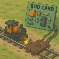
The BSD Card is an electronic circuit breaker for power districts. It provides short-circuit protection at the block level, similar in purpose to commercial PSX units but fully integrated with LCC.
Purpose: Protects wiring, boosters, and decoders by rapidly cutting power to a block when a short or overload occurs.
Configurable: CDI configuration for current thresholds for occupancy and short circuits.
Integration: Generates LCC events when track is occupied or a short occurs.
Connections: Installs between the booster/power supply and up to 4 blocks, one line per block.
May be used stand-alone for protection, or chained into a BOD Card (via short network cable) for combined protection + occupancy detection per block.
In hobbyist terms, the BSD is the “circuit breaker card” for your layout’s power districts. It performs the same role as a PSX (by DCC Specialties) or other electronic breaker, but with the added benefit of LCC event reporting and configuration.
| Card | Full Name | Purpose | Typical Placement |
|---|---|---|---|
| BOD | Block Occupancy Detection | Detects normal current draw (locos, cars with resistors, lights). Generates LCC events when a block is occupied. | Inline with each block’s Rail B via Breakout Board |
| BRD | Block Reversing Detection | Detects shorts at reverse loops or wyes. Coordinates polarity switching with a latching relay. | Between mainline and reversing section |
| BSD | Block Short Detection (was SCOD) | Provides per-block protection. Trips power when current exceeds selectable threshold (e.g., 1.5 A, 2.5 A, 3.5 A). Generates LCC events for trip, retry, and reset. | Inline with each block’s Rail B before BOD |
flowchart LR
  can("CAN / LCC Network");
  booster["Booster / Power Supply"]
  subgraph layout ["Train Layout"]
  bb1[["Block Breakout Board<br>(protection-only)"]]
  bb2[["Block Breakout Board<br>(protection/detection)"]]
  bb3[["Block Breakout Board<br>(detection-only)"]]
  tb1(("Track Block"))
  tb2(("Track Block"))
  tb3(("Track Block"))
  subgraph hub ["Node Bus Hub"]
    bod1[["BOD Card<br>(Daisy-Chained)"]]
    bod2[["BOD Card"]]
    bsd1[["BSD Card <br/>(Short Protection<br>4x Blocks)"]]
    bsd2[["BSD Card <br/>(Short Protection<br>4x Blocks)"]]
    nodeCard[[Node Card]]

    bsd1 -->|"Protected Power Outputs"| bb1
    bsd1 -.->|"Trip<br/>(GPIO Output)"| nodeCard

    bsd2 -->|"Protected Power Outputs"| bod1 --> bb2
    bsd2 -.->|"Trip<br/>(GPIO Output)"| nodeCard

    bod1 -->|"Occupancy<br>(GPIO Output)"|nodeCard
    bod2 -->|"Occupancy<br>(GPIO Output)"|nodeCard

 		bod2 -->bb3
  end
  	bb1 --> tb1
  	bb2 --> tb2
  	bb3 --> tb3
    nodeCard -->|"LCC Events <br/>(Trip & Occupancy Events)"| can
  end
    	booster -->|"Power In"| bsd1
    booster -->|"Power In"| bsd2
    booster -->|"Power In & <br>Non-Protected Power Outputs"| bod2


  %% Styles
  classDef lSalmonStyle fill:#FFA07A,stroke:#333,stroke-width:2px,font-size:22px;
  class bsd1,bsd2 lSalmonStyle;

  classDef lblueStyle fill:lightBlue,stroke:#333,stroke-width:2px,font-size:22px;
  class bod1,bod2 lblueStyle;

  classDef lyellowStyle fill:lightYellow,stroke:#333,stroke-width:2px,font-size:22px;
  class bod lyellowStyle;

  classDef lightGrayStyle fill:#d3d3d3,stroke:#333,stroke-width:2px,font-size:22px;
  class layout lightGrayStyle;

  classDef lGreenStyle fill:lightgreen,stroke:#333,stroke-width:2px,font-size:22px;
  class nodeCard lGreenStyle;
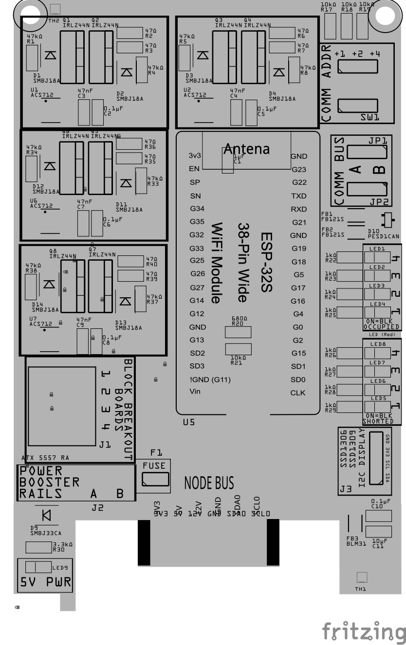
Assembly and Component Placement
This section combines both the component specifications and the assembly instructions to ensure a smooth assembly process. Below is a comprehensive list of components, their placement on the PCB, and orientation details to assist you during assembly.
High-Level Steps for Assembly:
- PCB for the card can be ordered from any PCB fabricator using these Gerber Files.
- Clean PCB with alcohol to remove residue. See Cleaning_PCB for details.
- See also: Soldering Tips
- PCB Components - listing of components used for PCB assembly
- PCB Parts - listing of parts used for PCB assembly
Below is a list of the PCB components used for this card (see diagram before reference):
![]()
![]()
| Component Identifier | Count | Type | Value | Package | Purpose | Orientation |
|---|---|---|---|---|---|---|
| Connectors | ||||||
| J1 | 1 | RJ45 Jack | 8-pin each | PTH | District outputs to Block Breakout. 4 blocks via network cable. odd pins = Rail B even pins = gapped Rail A, ) |
Keyed |
| J2 | 1 | ATX 5557 Header | 2-pin | PTH | Booster input: Rail A, Rail B | See PCB silkscreen labels |
| J3 | 1 | Female header | 2-Pin, 2.54mm | PTH | OLED Display Connection | None |
| Capacitors | ||||||
| C2, C4, C6, C8 | 4 | Capacitor-Ceramic | 0.1 µF | 1206 SMD | Noise filtering for ACS712 | None |
| C3, C5, C7, C9 | 4 | Capacitor-Ceramic | 47nµF | 1206 SMD | Decoupling for ACS712 and logic circuits | None |
| C10 | 1 | Capacitor-Ceramic | 0.1uF | 1206 SMD | Decoupling and noise reduction capacitor for I2C display | None |
| C11 | 1 | Capacitor-Ceramic | 10uF | 1206 SMD | Decoupling and noise reduction capacitor for I2C display | None |
| Diodes | ||||||
| D1-D8 | 8 | TVS Diode | SMBJ18A | SMB | Gate-to-source clamps, protect IRLZ44N gates | White bar towards PCB top edge |
| D9 | 1 | TVS Diode | SMBJ33CA | SMB | Protects track bus against voltage spikes during trip | None (bi-directional) |
| D10 | 1 | ESD Diode | PESD1CAN | SOT-23 SMD | I2C data bus electrostatic discharge (ESD) protection. | None |
| Filters & Noise Suppression | ||||||
| FB1, FB2, FB3 | 3 | Ferrite Bead | BLM31PG121SN1L | 1206 SMD | Noise suppression for I2C data lines and I2C display | None |
| F1 | 1 | Polyfuse (PPTC) | JK30, 3 A hold, 16 VDC (or more) (size for worst-case inrush; software trips ≤5 A.) |
5.1mm pitch, PTH | Auto-resetting overcurrent protection on Rail B input | None |
| Transistors | ||||||
| Q1 - Q8 | 8 | N-MOSFET | IRLZ44N, 55 VDC, 47 A | TO-220 | Back-to-back FETs to disconnect Rail B | Tab → Drain |
| Resistors | ||||||
| R2,R3,R6,R7, R10,R11,R14,R15 |
8 | Resistor | 47Ω | 1206 SMD | Gate resistors, limit ringing | None |
| R1,R4,R5,R8, R9,R12,R13,R16 |
8 | Resistor | 47kΩ | 1206 SMD | Gate pulldowns | None |
| R17-R19 | 3 | Resistor | 10kΩ | 1206 SMD | Current limiting for Comm Address Offset | None |
| R20 | 1 | Resistor | 680 Ω | 1206 SMD | Voltage Divider (high/low ends) | None |
| R21 | 1 | Resistor | 10k Ω | 1206 SMD | Voltage Divider (high/low ends) | None |
| R22-R29 | 8 | Resistor | 1kΩ | 1206 SMD | Current limiting for LEDs | None |
| R30 | 1 | Resistor | 3.3kΩ | 1206 SMD | Current limiting for LED | None |
| Indicators | ||||||
| LED1-LED4 | 4 | LED (Red) | 2 mA | 1206 SMD | Block Occupied | Reference back of LED, position cathode towards PCB left edge |
| LED5-LED8 | 4 | LED (Red) | 2 mA | 1206 SMD | Block Occupied | Reference back of LED, position cathode towards PCB left edge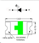 |
| LED9 | 1 | LED (Red) | 2 mA | 1206 SMD | 5V Power Indicator | Reference back of LED, position cathode towards PCB left edge |
| Selectors & Indicators | ||||||
| JP1, JP2 | 2 | Male Header | 3P, 0.1” spacing | PTH | Used for COMM BUS selection (I2C hardware bus) for either BUS A or BUS B. Must match LCC Node configuration (CDI). | None |
| SH1, SH2 | 2 | Jumper Cap | 2.54mm | N/A | Used with I2C Bus and Vcc selections. Recommend tall caps for ease of use. | None |
| SW1 | 1 | DIP / Slide Switch | 3P, 2.54mm | N/A | Used for COMM ADDR selection (I2C address offset, 0-7). | Position ON towards PCB top edge |
| ICs | ||||||
| U1-U4 | 4 | ACS712 | 20 A version | SOIC-8 | Measures block current for trip threshold and telemetry | Pin 1 (small dot) to Upper ride side of card |
| U5 | 1 | ESP32 Module | ESP32 DevKitC | DevKitC | Controller (BSD firmware) | Antenna clear |
| Miscellaneous | ||||||
| 1 | OLED Display | SSD1309, SSD1306 | 4-Pin, I2C | Display serial messages from firmware | Refer to silk screen of OLED and card, display extends out from card. |
Tools Required
For a list of recommended tools, refer to List of recommended tools.
Safety Precautions
- See Safety Precautions.
Testing and Verification
The following test and verifications of the card should be performed after a through inspection of the card’s soldering. Check all of the PTH component pins and SMD pads. Make sure there are no solder bridges between pins and pads.
Configure the BSD Card:
-
Select the
COMM BUSby positioning (2) Jumper Caps on eitherAorBmale header pins (JP1, JP2) -
Select the
COMM ADDRESSswitch (SW1) by sliding each of the 3 switches to either theONorOFFposition. Setting a switch to ON increments the address by 1, 2, or 4 for an address range of 0 to 7. Up to 8 devices can then be configured forAand 8 forB. -
Install the BSD Card’s firmware from
Visual Inspection
-
Initial Check: Examine the board for any obvious issues like missing components, solder bridges, or components that are misaligned or not fully seated.
-
Solder Joint Inspection: Use a magnifying glass or a microscope to inspect solder joints. Look for cold solder joints, insufficient or excessive solder, or any shorts between pads.
-
Component Orientation: the IC’s are correctly oriented according to the PCB silkscreen or schematic.
Power-Up Tests
- Seat the Audio Card Insert the Audio Card into a tested LCC Fusion Node Bus Hub (leave speakers disconnected).
- Load firmware & insert the ESP32
- Flash the Audio Card firmware onto an ESP32 DevKit-C.
- Insert the DevKit-C into the Audio Card’s socket.
- Power and open the self-test console (Audio Card’s ESP32)
- Power the Node Bus Hub using either a tested Node Card or a Power-CAN Card.
- Quickly check for hot components; power off if anything heats abnormally.
- Open a serial monitor at 115200 to the Audio Card’s ESP32 (DevKit-C on the Audio Card, not the Node Card).
- Enter
Tto start the self-test, then review the results.- Messages may appear on BT, OLED, or the attached serial monitor.
- See: PCB Self Testing.
- What you do: simply watch the summary—no meters or scopes required.
- Pass indicators: each tested group reports a success status.
- If any group fails: power down, re-seat the DevKit-C and Audio Card, inspect solder on the affected header/IC, and re-run.
- Audio Card Pins Test (automatic)
- I²S:
BCLK,LRCLK,DIN[1..4]driven and verified as Outputs. - SPI:
SCK,MOSI,CSas Outputs;MISOchecked as an Input. - I²C:
SDA/SCLbriefly exercised as open-drain I/O to confirm upstream Hub pull-ups and line integrity.
- I²S:
- SD Card Access Test (automatic)
- Initializes the SD interface at a conservative SPI clock, opens a small file, and reads a short block.
- What you do: insert a known-good micro-SD and observe init/read status.
- If it fails: try a different card, re-seat the socket, and re-run. (Lower SPI speed in firmware if needed.)
- Speaker Path Test (audible)
- Plays a short test-tone sequence over I²S → MAX98357A → speaker with gentle fade-in/out.
- What you do:
- Connect one speaker to the first speaker connector.
- Run the Speaker Test and listen for two distinct tones (e.g., higher tone then lower).
- For multiple amps/speakers, move the connector to each line and repeat.
- Expected result: clear, non-distorted tones at moderate volume; no pops/crackles at start/stop.
- If no sound: verify I²S header orientation, amplifier IC soldering, speaker wiring/polarity, and the 5 VDC audio rail.
Functional Testing
Functional testing of the card can be performed after completing the power-up testing. Testing consists of testing network communiations, followed by the sensing of current in a layout track block.
HW Communications Testing
Communications testing verifies the LCC Node can communicate with the BSD Card’s I2C IC via the Node Bus Hub connections. This is performed using the LCC Fusion Node Card’s testing firmware and a serial monitor.
-
Insert the BSD Card into a Node Bus Hub along with a LCC Fusion Node Card.
-
Install LCC Fusion Project firmware that includes serial monitor for testing.
-
Verify that the I2C connection between the LCC Fusion Node Card and the BSD Card work.
See Testing I2C Cards for details on how to test the communications for a I2C enabled card.
MCP IC Testing
After hardware communication has been established, to verify the MCP IC, use the Node’s serial monitor to simulate an input from each of card’s input pins as follows:
- In the serial monitor’s input, enter
Mfor the LCC Node’s serial monitor Main Menu. - Select
[1] Node Managementand[1] Device Testing Management - Select
[5] Simlulate MCP Device Input - From the list of MCP devices, select the device # for the BSD Card being tested
- Enter the number for the pin to tested.
- Using the JMRI LccPro event monitoring tool, verify the correct Event ID was issued.
Track Block Testing
After validating the LCC Fusion Node Card can communicate (find) the BSD Card, test each of the BSD Card block connections.
Track block detection verification is performed using a Block Breakout Board connected to a track block.
-
Connect a network cable (CAT5/6) to one of the BSD Card’s RJ45 connector.
- Connect the other end of the network cable to (1) Block Breakout Board.
- Connect one of the Test Track rails directly to the Track Bus VDC+ connection.
- Connect the other Test Track rails to one of the Block Breakout Board block connections (BLK1 - BLK4)
- Connect the Test Track Bus GND to the Block Breakout Board TRACK BUS GND connection
- Configure each of the card’s device lines using an LCC CDI Configuration Tool
- Open an LCC Event Monitoring tool (e.g. JMRI Event Monitoring tool).
-
Test each of the Breakout Board device connections using a locomotive (one at a time)
- draw current on the track by either
- placing a 10KΩ resistor across the track, or
- placing a locomotive on to the track
- Turn on the Track Power (let locomotive idle)
- Validate the configure Event ID for Block Occupied is sent by viewing the Event Monitoring tool
- draw current on the track by either
- Repeat testing for all (8) BSD Card connections as follows:
- Connect the Block Breakout Board to the first RJ45 socket (J1) for blocks 1-4.
- Reconnect to 2nd RJ46 socket (J2) for blocks 5-8.
Excellent — here’s your final, concise and production-ready Markdown section for the BSD Card Assembly Guide. It folds the setup steps into the procedure, adds the Tact Button 1–4 + LED checks, and trims all the “why” explanations for clarity and flow.
Block Short Detection Testing (Using Card Digital Input Controller Board)
Use the Card Digital Input Controller Board to verify all four BSD block inputs for both Occupancy and Short Detection using the built-in 10 kΩ load and Tact Buttons 1–4.
Procedure
-
Connect
- Plug the BSD Card’s RJ45 block input into the Card Digital Input Controller Board.
- Power the BSD Card from a tested Node Bus Hub.
- Turn Load Switch ON (10 kΩ).
- Set JP1 = LINE, JP2 = LINE, and J2 = CONNECTED to the Hub GND (required for LED power).
- Ensure tester VDC+ rail (3.3 VDC or 5 VDC) is active so LEDs light.
-
Open Serial Monitor at 115200 baud (YAT or Arduino IDE).
- Press ENTER once to reach the BSD prompt.
-
Run Occupancy Test
-
Enter:
< 1.0 5.0 1.0 5.0 1.0 5.0 1.0 5.0 > -
Press Tact Button 1 → 4, one at a time.
-
Verify each block’s LED lights when its button is pressed.
-
Check serial console or LCC messages report Block n = Occupied.
-
-
Run Short-Logic Test
-
Enter:
< 0.0 0.8 0.0 0.8 0.0 0.8 0.0 0.8 > -
Again press Tact Buttons 1 → 4, one at a time.
-
Verify each LED lights during button press.
-
Check serial console or LCC messages report Block n = Short Detected.
-
-
Repeat for any additional BSD Cards if testing multiple units.
-
Restore runtime thresholds after testing (normal short threshold ≈ 45 mA).
Quick Reference
| Test | Command | Expected Result |
|---|---|---|
| Occupancy | < 1.0 5.0 1.0 5.0 1.0 5.0 1.0 5.0 > |
Each Tact Button 1–4 lights its LED and reports Occupied |
| Short-Logic | < 0.0 0.8 0.0 0.8 0.0 0.8 0.0 0.8 > |
Each Tact Button 1–4 lights its LED and reports Short Detected |
Notes
- J2 GND must be connected for LEDs and buttons to operate.
- The 10 kΩ load remains floating across the block pair and does not reference GND.
- This verifies both logic paths safely without a high-current short fixture.
Provisioning the Card
- See Provisioning a Card.
Troubleshooting
- See I2C Trouble Shooting.
Appendences
PCB Specifications
Specifications for the card include:
![]()
| Characteristic | Value |
|---|---|
| Maximum BSD Detections | 4 |
| Maximum Block Breakout Board | 1 |
| Maximum Cards per LCC Fusion Node Cluster | 161 |
| Maximum Track Current | 3.5A2 |
| Minimum Track Voltage | 14.2 VDC3 |
| Max Track Voltage (determined by MCT6H IC) | 30 VDC |
- The LCC Fusion Node Cluster supports up to 16 cards, distributed across two I2C hardware buses, with a maximum of 8 cards per bus.
- The BSD Card uses 54mil PCB traces, to support up to 3.5A. The card also uses a 3.5A fuse.
- The minimum track voltage is 14.2 VDC due to the voltage drop from the bridge rectifier on the BSD Card (which reduces voltage by 2.2 VDC). DCC decoders require at least 12 VDC, in accordance with NMRA DCC standards.
How It Works
The BSD Card is an ESP32-based, polled I²C peripheral that senses block current and can disconnect Rail B on faults. The LCC Fusion Node Bus Hub provides 3V3, 5V, 12V, GND and the I²C bus. The producer polls the BSD Card roughly every 33 ms.
1) Blocks and the monitored rail
One layout rail—by convention, Rail B—is gapped to form blocks (approaches, turnouts, routes, etc.). The other rail (Rail A) is the return. A block is “occupied” when a loco or resistor-equipped car allows current to flow between A and B inside that gapped section.
Tip: cars with a ~10 kΩ wheelset resistor improve occupancy continuity across dirty track.
2) BSD wiring via the Breakout
Each BSD Card services four blocks through a single RJ45 to a Block Breakout Board. Your mapping is:
- Pins 1/3/5/7 = Rail A, Pins 2/4/6/8 = Rail B (one block per adjacent pin pair).
- All Rail B paths from the four blocks return through the BSD Card so current can be sensed and switched.
Current direction does not matter (ACS712 is bidirectional; firmware uses I ). Consistency does: keep all B legs routed through the BSD.
3) District current path (Rail B)
With the rail ON, the high-current path is:
Booster J1(B) → F1 (PPTC) → ACS712 IP+ → ACS712 IP− → Q1 Drain → Q1/Q2 Sources (switch node) → Q2 Drain → RJ45 even pins (2/4/6/8) → block → return on RJ45 odd pins (1/3/5/7) → Booster J1(A).
Both rails carry the same magnitude; size Rail A copper and Rail B copper equally.
4) Protection and power stage
- PPTC Fuse (F1, 3 A hold) limits sustained over-current upstream of sensing/switching.
- TVS across rails (D3, SMBJ33CA, bidirectional) clamps transients at the RJ45.
- Back-to-back MOSFETs (Q1/Q2) disconnect Rail B in either polarity.
- R1/R2 (47 Ω) per gate (at FET end) limit dI/dt and damp ringing.
- R3/R4 (47k) from each gate→source (FET-side of R) ensure OFF at reset.
- D1/D2 (SMBJ15A, unidirectional) clamp G-S surges on the FET-side of Rg.
- ACS712 decoupling: 0.1 µF + 1 µF at VCC-GND; C_FILT 47 nF from FILTER→GND sets ~2 kHz internal bandwidth.
5) Sensing and occupancy
- The ACS712 VOUT is read by an ADC1 pin on the ESP32.
-
Firmware averages samples, applies a light IIR filter, and treats the magnitude I (sign ignored). - Occupied is true when filtered current ≥ your OCC threshold (gentle, below the short level).
6) Short detection and automatic retry
Each line runs a small state machine:
- Inrush blanking: after power-up and each re-enable, ignore short checks until t_unblank (configurable ms) to avoid false trips on inrush.
- Trip: if filtered current ≥ short trip level (from CDI selection, e.g., 0.5…5 A) outside the blanking window, the BSD opens Rail B (gates LOW) and flags SHORT.
- Retry: after a delay stage (e.g., 300 ms → 1 s → 3 s), the BSD briefly reconnects. It takes a fresh sample; if current is still high, it re-trips and advances the stage.
- Lockout: after the configured number of retries, the line remains OFF until reset (host command or power-cycle).
7) I²C reporting (polled)
- The BSD is an I²C target at I2C_BASE_ADDR=0x58 + DIP(0..7).
- On each read, it returns 2 bytes: byte 0 = OCC bitmask, byte 1 = SHORT bitmask (lines 0..7).
- The Node producer polls each BSD Card (≈33 ms cadence) and issues layout events based on these masks.
8) Indicators (active-low)
- Occupied LEDs and Short LEDs are tied 3V3 → R (≈1 k) → LED → GPIO.
- LOW = LED ON, HIGH/Hi-Z = OFF.
- On strap pins (e.g., GPIO0/2/4/5/12/15), this active-low wiring is boot-safe; only drive them after startup.
Connections
The purpose of the BSD Card is to provide detection of track block occupancy by detecting current.
![]()
| Component Designator | Connector Label | Connector Type | Connection Number | Description | | ——————– | ——————– | ————– | ——————— | ———————————————————— | | J1 | BLOCK BREAKOUT BOARD | RJ45 Socket | 1/2, 3/4, 5/6, 7/8 | Use a network cable to connect to the Block Breakout Board ** which connects to the track blocks. | | **J2 | POWER BOOSTER RAILS | ATX 5557 RA | A, B | Use to connect to power booster use 12-16 AWG wiring |
PCB Protection
To ensure the reliable operation and longevity of your BSD Card, several protection components have been integrated. These components safeguard the BSD Card from overcurrent, voltage spikes, and electrical noise. Below is a brief overview of each protection element and its role:
![]()
| Protected Component | Protection Component | Function | Specifications | Location |
|---|---|---|---|---|
| LEDs (occupied/short) | Series resistor | Limits LED current (dim indoor level) | 1 kΩ, 1% (gives ~0.3–1.3 mA @3.3 VDC depending on LED Vf) | Active-low: 3V3 → R → LED → GPIO (at MCU side) |
| ACS712 (U1) VCC | Decoupling capacitors | Stabilize supply; shunt HF noise | 0.1 µF X7R + 1 µF bulk (can share bulk on local 5 VDC rail) | Directly across VCC–GND at U1 (short return) |
| ACS712 (U1) FILTER | Bandwidth (FILTER) capacitor | Reduces output noise; sets internal LPF | 47 nF (tune 10–100 nF as needed) | FILTER → GND at U1 (very close) |
| MOSFET gates (Q1/Q2) | Gate series resistors (Rg1/Rg2) | Limit gate surge, damp ringing, improve EMI | 33–47 Ω, 1/10 W, one per gate | In series from GPIO to each gate; place at FET end |
| MOSFET gates (Q1/Q2) | Gate pulldowns (Rp1/Rp2) | Ensure OFF at reset; resist Miller turn-on | 47–100 kΩ from gate→source (FET side of Rg) | Next to each MOSFET |
| MOSFET gates (Q1/Q2) | G-S TVS clamp | Protects gate oxide from ESD/transients | SMBJ15A (unidirectional), DO-214AA (SMB) | Across Gate–Source, FET side of Rg |
| Track rails (A↔B at RJ45) | Rail TVS | Clamps trip/transient spikes on the cable | SMBJ33CA (bidirectional), DO-214AA (SMB) | Across A↔B near RJ45 (J2) with short, symmetric paths |
| Rail-B path (entire board) | Resettable fuse (PPTC) | Limits sustained overcurrent upstream of sense & switch | JK30, 3 A hold (evaluate to suit inrush/thermal) | J1(B) → PPTC → ACS712 IP+ (in series) |
| I2C (SDA/SCL), I2C Display | Ferrite beads | Suppress HF noise on bus lines | BLM31PG121SN1L, 120 Ω @ 100 MHz | In series with SDA and SCL, near card edge |
| I²C (SDA/SCL) | ESD diodes | Protect bus from ESD to chassis/ground | Low-cap ESD, e.g., PESD5V (Vr≈5 VDC), SOD-323/SOT-23 | From SDA→GND and SCL→GND, close to ESP32 pins |
References
ESP32 GPIO Mapping
| BSD Card Function | GPIO Pin | Node Card Function | GPIO Pin |
|---|---|---|---|
| I2C SDA | 19 | I2C SCL | 18 |
| Block Current Sensing (ADC)(ACS VOUT) | 36, 39, 34, 27 | Block Relay (IRL Gate) | 32, 16, 33, 25 |
| Block Occupied LEDs | 17, 5, 0, 4 | Block Shorted LEDs (5v) | 15, 2, 12, 14 |
| HARDWARE DETECTION (voltage divider determine which card is present) (Input) | 13 | ||
| Flash Pins (reserved) | 6, 7, 8, 9, 10,11 | UART0 (reserved) | 1, 3 |