Button Card Assembly Guide
Table of contents
Table of contents
Introduction
See the How to Use Assembly Guides for detailed instructions.
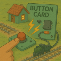
In conjunction with the LCC Fusion Node Card and a Node Bus Hub, the Button Card provides input control for up to 16 separate buttons. Typically when used for input in an LCC Node arrangement, this card can be attached to input buttons to have the an LCC Node produce LCC Events of on/off. These events are subsequently consumed by a LCC Node to accurately control the functioning states of the other output devices.
flowchart LR;
can["CAN Network"];
subgraph layout ["Train Layout"];
direction LR;
b["Button Device (16x)"] --> |"Button Press<br/>(on/off)"| bb[Digital I/O  Breakout Board];
bb --> |"Digital Input <br/> (high/low)"| c["Button Card (16x)"];
c -->|"GPIO Output <br/> (high/low)"| n[Node Card];
n -->|"LCC Event<br/>(on/off)"| can;
end;
classDef lSalmonStyle fill:#FFA07A,stroke:#333,stroke-width:2px,font-size:24px;
class c lSalmonStyle;
classDef lightGrayStyle fill:#d3d3d3,stroke:#333,stroke-width:2px,font-size:24px;
class layout lightGrayStyle;
Assembly and Component Placement
This section combines both the component specifications and the assembly instructions to ensure a smooth assembly process. Below is a comprehensive list of components, their placement on the PCB, and orientation details to assist you during assembly.
High-Level Steps for Assembly:
- PCB for the card can be ordered from any PCB fabricator using these Gerber Files.
- Clean PCB with alcohol to remove residue. See Cleaning_PCB for details.
- See also: Soldering Tips
- PCB Components - listing of components used for PCB assembly
- PCB Parts - listing of parts used for PCB assembly
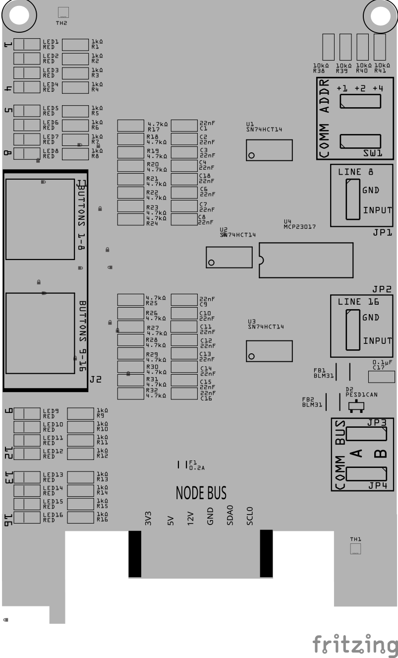
Below is a list of the PCB components used for this card (see diagram before reference):
![]()
![]()
| Component Identifier | Count | Type | Value | Package | Purpose | Orientation |
|---|---|---|---|---|---|---|
| Capacitors | ||||||
| C1 - C16 | 16 | Capacitor-Ceramic | 22nF | 1206 X7R | Low-Pass Filter to filter out noise and prevent unwanted transient signals | None |
| C17, C18 | 1 | Capacitor-Ceramic | 0.1uF | 1206 X7R | Decoupling capacitor for IC protection. | None |
| Diodes | ||||||
| D1 | 1 | ESD Diode | PESD1CAN | SOT-23 SMD | I2C data bus electrostatic discharge (ESD) protection. | Fits only one way |
| F1 | 1 | Fuse-PTC Polymer | PPTC, 0.2A | 1206 SMD | Protects from sustained overcurrent conditions | None |
| Filters & Noise Suppression | ||||||
| FB1, FB2 | 2 | Ferrite Bead | BLM31PG121SN1L | 1206 SMD | I2C network bus data line noise suppression. | None |
| Connectors | ||||||
| J1, J2 | 2 | RJ45 Socket | 8P8C | N/A | Network cable (CAT5/6) connection to I/O breakout board connected to buttons. | Fits only one way |
| Resistors | ||||||
| R1 - R16 | 16 | Resistor | 1kΩ | 1206 SMD | Current limiting for LED1 - LED16 | None |
| R17-R32 | 16 | Resistor | 4.7kΩ | 1206 SMD | Low-Pass Filter to filter out noise and prevent unwanted transient signals | None |
| R38 - R41 | 4 | Resistor | 10kΩ | 1206 SMD | Used by switch SW1 to pullup the MCP23017 for I2C address. | None |
| Selectors & Indicators | ||||||
| JP1, JP2 | 2 | Male Header | 3P, 0.1” spacing | N/A | Used for LINE 8 and LINE 16 selection of either GND or INPUT. Set to GND when button require this card to provide the circuit’s GND connection. |
None |
| JP3, JP4 | 2 | Male Header | 3P, 0.1” spacing | N/A | Used for COMM BUS selection (I2C hardware bus) for either A or B. Must match the configuration within the LCC Node (CDI). |
None |
| SH1 - SH4 | 4 | Jumper Caps | 2.54mm | N/A | Used with I2C Bus and LINE 8/16 selections. Recommend tall caps for ease of use. | None |
| Switches & Indicators | ||||||
| SW1 | 1 | DIP / Slide Switch | 3P, 2.54mm | N/A | Used for COMM ADDR selection (I2C address offset, 0-7). Up to 8 cards can be installed per I2C bus. Must match the LCC Node configuration (CDI). | Position ON towards PCB top edge |
| LED1-LED16 | 16 | LED | Red | 1206 SMD | Indicates button has been pressed | |
| ICs | ||||||
| U1, U2, U3 | 3 | IC (Schmitt Trigger) | SN74HCT14 | DIP-14 PTH | Contains 6 triggers to transform noisy or slow-changing input signals into clean, fast digital outputs. | Position IC’s dimple (pin 1) towards PCB left edge |
| U4 | 1 | IC (GPIO expander) | MCP23017 | SSOP28 | I/O expander using I2C serial interface to control 16 GPIO pins. | Position IC’s dimple (pin 1) towards PCB left edge |
| U5 | 1 | EEPROM | AT24C02 | SOIC-8 | Memory for card’s type and description | IC indent is positioned towards PCB bottom edge |
Tools Required
Safety Precautions
- See Safety Precautions.
Testing and Verification
Configure the card:
- Select the I2C bus (COMM BUS) by positioning (2) Jumper Caps on either BUS A or BUS B male header pins (JP1, JP2)
- Select the I2C address (COMM ADDR) switch (SW1) by slide each of the 3 switches to either the ON or OFF position. Setting a switch to ON increments the address by 1, 2, or 4 for an address range of 0 to 7. Up to 8 devices can then be configured for BUS A and 8 for BUS B.
Visual Inspection
-
Initial Check: Examine the board for any obvious issues like missing components, solder bridges, or components that are misaligned or not fully seated.
-
Solder Joint Inspection: Use a magnifying glass or a microscope to inspect solder joints. Look for cold solder joints, insufficient or excessive solder, or any shorts between pads.
-
Component Orientation: the IC’s are correctly oriented according to the PCB silkscreen or schematic.
Connectivity Testing
Power-Up Tests
- Assembly a tested Power Module to the LCC Fusion Node Card.
- Apply Power to the Power Module and verify the following:
- Check for Hot Components: Feel for components that are overheating, which could indicate a problem like a short circuit or incorrect component.
Testing Using the Card Input Control Board
This procedure verifies that the Button Card correctly detects button presses (active-LOW inputs) when tested with the Card Input Control Board (CICB). Each tact switch on the board safely pulls one of the card’s lines to GND when pressed. The test confirms that all of the card’s input lines respond as expected and that LCC Events are sent and/or messages appear on the Serial Monitor.
Required Items:
- Tested LCC Fusion Node Bus Hub
- Button Card seated in the Hub
- Card Input Control Board
- CAT-5/6 network cable (RJ45)
- USB Cable for serial monitor
- Serial Monitor (YAT, Arduino IDE, or WebSerial) Baud rate = 115 200
Setup and Connections
- Use a network cable to connect the Button Card to the Card Input Control Board
- Select both the Button Card’s Line 8 (and 16) selector and the Card Input Control Board selector to match:
- Select INPUT when testing with a common GND connected to the Card Input Control Board (i.e. testing the line for input)
- Select GND when testing without a GND connected to the Card Input Control Board
Power and Firmware
- Power the Hub using a tested Node Card loaded with firmware
- Connect USB to your computer and open the Serial Monitor at 115 200 baud.
- Wait for the Node Card to complete initialization.
Testing
- Press each of the Card Input Control Board buttons:
- the corresponding Button Card LED should turn on
- a message is displayed on the serial console when in testing mode (serial input command
Twas previously entered) - a LCC Event will be sent by the Node Card and display in an LCC Event viewer (if configured)
Provisioning the Card
- See Provisioning a Card.
Troubleshooting
- See I2C Trouble Shooting.
Appendences
PCB Specifications
Specifications for the card include:
![]()
| Characteristic | Value |
|---|---|
| Max Buttons | 16 |
| Maximum Number of Cards per LCC Fusion Node Cluster | 161 |
- The LCC Fusion Node Cluster can support up to 16 cards, distributed across two I2C hardware buses, with a maximum of 8 cards per bus.
- Note: total includes all cards using the I2C address range of
0x20(MCP23017 IC).
- Note: total includes all cards using the I2C address range of
- GND, 5V, 12 VDC (optional), SLA0/SDA0, and SDA1/SCL1 (optional)
How It Works
The Button Card provides up to 16 independent button inputs via a single MCP23017 I²C port expander. Each input line is wired through a clean-up buffer and uses internal pull-ups to detect individual button presses.
-
I2C & MCP23017 Initialization
- On power-up, the Node Firmware configures the MCP23017 over I2C. Address pins determine the expander’s I²C address.
- All 16 GPIO pins (GP0–GP15) are set as inputs with internal 3.3 V pull-ups enabled.
-
Button Inputs (Lines 1–16)
- Each of the 16 MCP23017 inputs connects to a corresponding pushbutton on the RJ45/ribbon header through a Schmitt-trigger buffer (e.g., 74HC14) for clean edges and improved bounce tolerance.
- Press = line pulled LOW → MCP23017 reads LOW → firmware emits LCC Event: Button ON.
- Release = line returns HIGH via pull-up → firmware emits LCC Event: Button OFF.
Ground Return (per 8-line group)
For each of the two 8-line groups (RJ45 sockets), the Line-8 selector on the Button Card and the Line-8 selector on the Digital I/O Breakout Board must be set the same. Choose one configuration to guarantee a single GND path (no loops):
GND Source Button Card (Line 8) Digital I/O Breakout (Line 8) Result Node Card’s GND (via Node Bus Hub) JP1 = GND
JP2 = GNDJP1 = GND Line 8 carries common return; Lines 1–7 are inputs. Layout-bus GND (from Breakout Board) JP1 = I/O
JP2 = I/OJP1 = I/O All 8 lines stay I/O; bring a separate GND wire from the Breakout Board. Do not mix states (e.g., Button Card = GND while Breakout = I/O). Pick one row and match both selectors for that 8-line group.
Quick wiring examples
- Option A (Line 8 = GND): Tie each button’s other lead to Line 1–7; Line 8 is the common return on the same cable.
- Option B (Line 8 = I/O): Bring GND from the Digital I/O Breakout Board (connects to the layout-bus GND); use Lines 1–8 for signals.
-
LED Indicators (Optional)
- For visual feedback, each button line can drive an LED: wire the LED anode to 3.3 V, the cathode through a 1 kΩ resistor to the Schmitt‑trigger output (pre-expander).
- When the button closes, the buffer output pulls LOW, lighting the LED until the button is released.
-
Debounce & Filtering
- *Purpose: The filter prevents false triggering from mechanical bounce (rapid on/off flicker when a button is pressed or released) and filters out high-frequency noise.
- How it works: When a button is pressed or released, the contact may momentarily vibrate or bounce, producing a noisy signal. The RC network—composed of a **10 kΩ series resistor and a 10 nF capacitor to ground—slows down these fast voltage changes. This forms a low-pass filter with a time constant (τ) of 0.1 ms, which smooths out spurious transitions.
- The SN74HCT14 Schmitt-trigger buffer further sharpens the resulting signal by introducing hysteresis, ensuring only clean HIGH or LOW levels are passed to the MCP23017.d
-
LCC Node Operation:
-
The firmware configures the MCP23017 port expander with internal pull-up resistors (set to 3.3 VDC). When an input device (such as a switch) pulls an input line to LOW (GND), the corresponding GPIO line of the port expander is pulled to LOW.
-
When the LCC Node firmware detects a GPIO state change to LOW, it generates an LCC Event to indicate the ON state. When the input device resets (e.g., the button is released), the GPIO line returns to HIGH, and the firmware generates an LCC Event for the OFF state.
-
PCB Protection
The Button Card provides detection of button presses. The following is an overview of each protection component integrated into the Button Card and its role:
![]()
| Protected Component | Protection Component | Function | Specifications | Location |
|---|---|---|---|---|
| Entire Card | PPTC Polyfuse | Protects from sustained overcurrent conditions by increasing resistance when the current exceeds 1.5A and 3A. Resets once the fault condition is cleared. | Hold Current: 500 mA | In series with the incoming Power line |
| MCP23017 IC | Decoupling Capacitors | Filters out high-frequency noise and transient voltage spikes from the power supply, ensuring stable voltage to MCP23017 IC. | Values: 0.1 µF ceramic | Across Vcc and GND near IC. |
| I2C Lines | Ferrite Bead BLM31PG121SN1L | Provides high-frequency noise suppression on the I2C lines. | Impedance: 120 ohms at 100 MHz | In series with the SDA and SCL lines of the I2C bus |
| I2C Lines | ESD Protection Diode PESD1CAN | Protects the I2C lines from electrostatic discharge and voltage spikes. | Reverse Stand-off Voltage (Vr): 24 VDCClamping Voltage (Vc): 40 VDC | Across the SDA and SCL lines to GND |
| Button Lines | RC Filter + Schmitt Buffer | Reduces EMI, contact bounce, and long-wire interference | Value: 22nF, 4.7kΩ | Inline series resistor, with cap between input line and GND |
References
-
I2C GPIO Mapping (Button Card)
RJ45 Line MCP23017 Pin GPIO Line Direction Pull-up Logic Levels Purpose Notes L1 GPA0 GP0 Input Enabled LOW = Pressed Button state reading Detects LOW when button pressed L2 GPA1 GP1 Input Enabled LOW = Pressed Button state reading L3 GPA2 GP2 Input Enabled LOW = Pressed Button state reading L4 GPA3 GP3 Input Enabled LOW = Pressed Button state reading L5 GPA4 GP4 Input Enabled LOW = Pressed Button state reading L6 GPA5 GP5 Input Enabled LOW = Pressed Button state reading L7 GPA6 GP6 Input Enabled LOW = Pressed Button state reading L8 GPA7 GP7 Input Enabled LOW = Pressed Button state reading May be used for GND detection