Digital I/O Breakout Board Assembly Guide
Table of contents
Table of contents
Introduction
The Digital I/O Breakout Board is a key component of the LCC Fusion automation system, designed to control up to eight digital I/O devices in model railroad applications and other low-power, precision movement tasks.
Working in conjunction with the LCC Fusion Node Card and either the Node Card ** or **Digital I/O Card, this breakout board receives control signals over a standard network cable via the onboard MCP23017 GPIO expansion controller. Each digital I/O device connects directly using a standard 3-pin JST XH connector (Signal, 5V, GND), simplifying installation with many types of devices for both input or output.
The board is powered by the layout’s accessory power bus (AC or DC), which is routed through an onboard bridge rectifier and regulated down to 5V using a voltage regulator. This provides a stable power supply for all eight digital I/O devices and the control circuitry.
flowchart LR;
subgraph layout ["Train Layout"];
n[["Node Card"]];
c[["Digital I/O  Card"]];
direction LR;
n <--> c;
n <--> bb;
c --> bb[Digital I/O <br/> Breakout Board];
bb --> m(("Digital Input / <br/> Output Devices(8)"));
end;
classDef lSalmonStyle fill:#FFA07A,stroke:#333,stroke-width:2px,font-size:20px;
class bb lSalmonStyle;
classDef lightGrayStyle fill:#d3d3d3,stroke:#333,stroke-width:2px,font-size:24px;
class layout lightGrayStyle;
System Overview:
The Digital I/O Breakout Board acts as an interface between the LCC Fusion Digital I/O Card and a variety of digital devices used in model railroad automation, including sensors, buttons, LEDs, and small actuators. It supports both digital inputs and digital outputs on its eight lines.
Diagram Overview:
The diagram below illustrates the flow of control signals and power between the components in the Digital I/O Breakout Board system:
- LCC Node Card: Receives LCC Events and manages configuration
- Digital I/O Card: Generates digital output signals, reads input digital input levels.
- Digital I/O Breakout Board:
- Accepts 5V-regulated power from layout power bus (AC/DC/DCC)
- Connects to up to 8 digital devices using 3-pin JST headers
flowchart LR;
subgraph layout ["Train Layout"];
  direction LR;
  can["CAN Network"];
  can2["CAN Network"];
  nodecard[["Node Card"]];
  nodecard2["Node Card"];
  c[["Digital I/O Card (16x)"]];
  c2[["Digital I/O Card (16x)"]];
  bb[[Digital I/O <br>Breakout Board]];
  out(("Output Device (16x)"));
  in(("Input Device (16x)"));
  bb2[["Digital I/O <br>Breakout Baord"]];

  can --> |"LCC Event<br/>(on/off)"| nodecard;
  nodecard -->|"GPIO Input <br/> (High/Low)"| c;
  c --> |"Digital Output<br/>(high/low)"| bb;
  bb --> |"Digital Output <br/> (high/low)"| out;

  in --> |"Digital Input <br/> (high/low)"| bb2;
  bb2 --> c2;
  c2 --> |"Digital Input <br/> (high/low)"| nodecard2;
  nodecard2 --> |"LCC Event<br/>(on/off)"| can2;
end;
classDef lSalmonStyle fill:#FFA07A,stroke:#333,stroke-width:2px,font-size:24px;
class c,c2 lSalmonStyle;
classDef lightGrayStyle fill:#d3d3d3,stroke:#333,stroke-width:2px,font-size:24px;
class layout lightGrayStyle;

acc["AC or DCC<br/>Accessory Power"];
acc --> |"5V"| bb
acc --> |"5V"| bb2
Control Flow
- LCC Event:
- The system begins when an LCC Event is sent over the CAN Network. This event may command changes such as activating an output device or requesting status from an input device.
- Node Card:
- The Node Card receives the LCC Event and processes it accordingly.
- For output events, the Node Card sends GPIO control signals to the Digital I/O Card to drive devices.
- For input events, the Node Card listens for status signals coming from the Digital I/O Card.
- Digital I/O Card:
- The Digital I/O Card, connected to the Node Card via network cable, manages digital I/O through the MCP23017 GPIO expander.
- In output mode, the Digital I/O Card converts the Node Card’s commands into GPIO output signals to control devices.
- In input mode, it reads digital input signals from devices and reports their states back to the Node Card.
- Digital I/O Breakout Board:
- The Breakout Board receives digital output signals from the Digital I/O Card and powers connected output devices.
- It also routes digital input signals from connected input devices back to the Digital I/O Card.
- Powered by the layout’s 5 VDC accessory bus, regulated via an onboard LM7805CV voltage regulator, ensuring stable power supply for all connected devices.
- Digital I/O Operation:
- For output devices, the Breakout Board drives the device control lines according to the GPIO output states.
- For input devices, it passes the device signal states through to the Digital I/O Card’s MCP23017 inputs, enabling the Node Card to receive status updates.
Assembly and Component Placement
This section combines both the component specifications and the assembly instructions to ensure a smooth assembly process. Below is a comprehensive list of components, their placement on the PCB, and orientation details to assist you during assembly.
High-Level Steps for Assembly:
- PCB for the card can be ordered from any PCB fabricator using these Gerber Files.
- Clean PCB with alcohol to remove residue. See Cleaning_PCB for details.
- See also: Soldering Tips
- PCB Components - listing of components used for PCB assembly
- PCB Parts - listing of parts used for PCB assembly
![]()
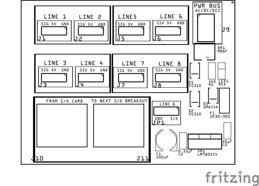
![]()
| Component Identifier | Count | Type | Value | Package | Purpose | Orientation |
|---|---|---|---|---|---|---|
| Bridge Rectifiers | ||||||
| BR1 | 2 | Bridge Rectifier | MB6F | SOP-4 | Converts DCC pulsating AC-like waveform into a DC-like pulsating waveform for current detection. | Position IC’s indent to PCB bottom edge (pin1 DC-) |
| Capacitors | ||||||
| C1 | 1 | Capacitor-Polymer | 100 uF | 6.3x5.8mm SMD | Smooths rectified DC voltage | See silk screen image |
| C2 | 1 | Capacitor-Ceramic | 0.33µF | 1206 X7R | Used by 5V voltage regulator for input filtering. | None |
| C3 | 1 | Capacitor-Ceramic | 22 uF | 1206 X7R | Used by 5V voltage regulator for output filtering. | None |
| Diodes | ||||||
| D1, D2 | 2 | Diode-Schottky | SS310 | SMA | Required | Protects against reverse current |
| D3 | 1 | TVS Diode | SMAJ5A | SMB SMD | Clamps voltage spikes on the 5 V line to protect breakout board and Digital I/O Card | Cathode end has a white line and positioned towards PCB bottom edge |
| Fuse | ||||||
| F1 | 1 | PTC Polymer Fuse | JK30, 1.5 A, 16 VDC (or more) | 5.1mm pitch, PTH | Resettable 1.5 A fuse for 5 V output protection | None |
| Connectors | ||||||
| J1 - J8 | 8 | Male Header | 3P, 2.54mm | n/a | Use to connect to digital I/O device SIG, 5V, GND | None |
| J9 | 1 | Connector | JST XH (2P) | 2.54mm | Connector to PWR BUS connections | Position connection towards PCB top edge |
| J10, J11 | 1 | RJ45 Socket | 8P8C | PTH | Network cable (CAT5/6) connection from Digital I/O Card and to 2nd Digital I/O Breakout Board | Fits only one way |
| Indicators | ||||||
| LED1 | 1 | LED | Red | 1206 SMD | Power indicator | Reference back of LED, position cathode towards PCB left edge |
| Resistors | ||||||
| R1 | 1 | Resistor | 1KΩ | PTH | Current limiting for power LED | None |
| Voltage Regulators | ||||||
| VR1 | 1 | Voltage Regulator | LM7805CV | TO-220 SMD | Provides 5V to digital I/O devices | Position heat sink towards PCB top edge |
Tools Required
Safety Precautions
- See Safety Precautions.
Testing and Verification
Visual Inspection
- Initial Check: Examine the board for any obvious issues like missing components, solder bridges, or components that are misaligned or not fully seated.
- Solder Joint Inspection: Use a magnifying glass or a microscope to inspect solder joints. Look for cold solder joints, insufficient or excessive solder, or any shorts between pads.
Functional Testing
Troubleshooting
- See I2C Trouble Shooting.
Appendences
PCB Specifications
Specifications for the Digital I/O Breakout Board include:
| Characteristic | Value |
|---|---|
| Max Devices | 8 |
| Output | 5V |
| Max Output1 | 1.5A |
| Maximum Number of Digital I/O Breakout Boards perI/O Card | 2 |
- Max current across all digital I/O devices is based on the LM7805 voltage regulator and fuse.
How It Works
The Digital I/O Breakout Board serves as the interface between the Digital I/O Card and various digital devices such as sensors, buttons, LEDs, and small actuators.
Signal Flow Overview
- The Digital I/O Card’s MCP23017 GPIO expander controls and monitors up to 16 digital lines, half of which can be routed to this breakout board via network cable.
- Each of the breakout board’s 8 lines connects to a device through a 3-pin JST XH connector, carrying Signal, 5 VDC power, and Ground.
Power Management
- The breakout board receives power from either:
- Output Card (or Node Card I/O) via LINE 7 and LINE 8
- Layout power bus (AC, DC, or DCC) from the layout power bus.
- When using the layout power bus:
- power is converted by the onboard bridge rectifier into a consistent DC polarity.
- A 5 VDC regulator (LM7805) then supplies stable voltage to power connected input devices and the board circuitry.
Device Interface
- Input Devices (e.g., sensors, switches):
Devices powered by 5 VDC from the regulator send digital HIGH/LOW signals via the Signal line to the MCP23017 configured as inputs. - Output Devices (e.g., LEDs, relays):
The MCP23017 outputs digital HIGH/LOW signals on the Signal line to control connected devices. The devices share the common 5 VDC power and ground reference.
Signal Integrity and Protection
- The Digital I/O Card provides series resistors and ESD protection near the MCP23017 pins.
- The breakout board is designed for straightforward wiring and minimal additional protection, relying on the Digital I/O Card’s robust safeguards.
- The 3-pin connector pinout ensures consistent device wiring:
- Pin 1: 5 VDC power
- Pin 2: Signal line
- Pin 3: Ground (common GND plane with either the layout power bus or the connected LCC Card (Node Card power supply))
Overall Operation
- The Node Card sends LCC events over the CAN network to the Digital I/O Card.
- The Digital I/O Card translates these events into digital I/O commands or reads, forwarding signals to/from the breakout board.
- The breakout board facilitates simple plug-and-play connection of common digital devices, enabling flexible and scalable automation control on the layout.
PCB Protection
The Digital I/O Breakout Board includes several key protection mechanisms to safeguard both the board itself and the connected components. Below is a detailed table outlining the protection provided against flyback voltage and reverse voltage, ensuring the longevity and reliability of your setup.
| Protected Component | Protection Component | Function | Specifications | Location |
|---|---|---|---|---|
| 5 VDC Power Rail | PTC Resettable Fuse (JK30 1.5 A) | Protects against overcurrent and short circuits on power input. | - Hold Current: 1.5 A - Voltage Rating: ≥6 VDC - Resettable fuse |
In series on power input (J9) |
| **5 V Regulator Output ** | TVS Diode (SMAJ5A) | Clamps voltage spikes on the 5 V line to protect logic and servos. | - Breakdown: ~6.4 V- Clamping: ~9 V- Unidirectional | Across 5 V rail and GND (after regulator output) |
| 5 VDC Power Input & Regulator | Bridge Rectifier | Ensures correct polarity and allows AC, DC, or DCC power while blocking reverse input. | - Max Input Voltage: 600 VDC AC - Avg Forward Current: ≥1 A - Forward Voltage Drop: ~1.1 VDC per diode |
Between accessory PWR BUS and regulator input |
| Dual 5 VDC Sources (Line 7 vs. Local Regulator) | Schottky Diodes (D1/D2, SS310) | Prevents back feeding between LCC card’s 5 VDC (Line 7) and local 5 VDC regulator | Vf ≈ 0.3–0.4 VDC @ 100 mA, 1–3 A IF, 40–100 VDC VR | Anode from each 5 VDC source, cathodes tied together to breakout +5 VDC rail |
| LM7805 Voltage Regulator | Input/Output Capacitors | Stabilizes voltage and suppresses regulator oscillation and ripple. | - Input: 0.33 µF ceramic + 220 µF electrolytic - Output: 0.1 µF ceramic + 220 µF electrolytic |
Close to regulator pins: IN ↔ GND, OUT ↔ GND |
| MCP23017 Signal Lines | Selectable 1 kΩ Series Resistors | Limits current to protect MCP23017 I/O pins from shorts and transient faults. | - Resistance: 1 kΩ ±5% - Power Rating: 0.125 W typical |
On Digital I/O Card, before MCP pins |
| MCP23017 Signal Lines | PESD1CAN ESD Protection Diodes | Protects MCP23017 pins from Electrostatic Discharge and voltage spikes. | - Working Voltage: 5 VDC - Peak Pulse Power: 1500 W (8/20 µs waveform) |
On Digital I/O Card, near MCP pins |