Digital Sensor Breakout Board Assembly Guide
Table of contents
Table of contents
Introduction
The Digital Sensor Breakout Board is a versatile accessory for the LCC Fusion Node Card, designed to provide up to six general-purpose digital connections. Each I/O line can be configured in firmware as either a digital input or a digital output, making the board suitable for a wide variety of layout control and sensing applications.
For inputs, the board supports sensors and devices such as capacitive touch modules, Hall effect switches, mechanical push buttons, and other logic-level devices.
For outputs, it can drive panel LEDs, relay triggers, or signal lines for external logic devices.
Each I/O line is available through a 3-pin header labeled V (3.3 V), S (Signal), and G (Ground). The signal line connects directly to a GPIO on the Node Card, and includes a built-in 1 kΩ series resistor for added protection. This keeps the design simple and robust while allowing safe connection of a wide range of 3.3 V-compatible devices.
The board connects to the Node Card using a standard RJ45 cable, with six GPIO lines and power shared across the connection. It requires no additional interface or hub, making it ideal for compact, distributed applications. For more complex systems, additional Digital Sensor capabilities can be added using I²C-based expansion cards via the Node Bus Hub.
With its flexible I/O support and simple plug-and-play wiring, the Digital Sensor Breakout Board is an essential building block for interactive and responsive model railroad layouts.
flowchart TD;
subgraph layout ["Train Layout"];
  direction LR;
  can["CAN Network"];
  can2["CAN Network"];
  sensor1(("Touch Sensor (6x)"));
  output1(("LED Output (6)"));
  nodecard[[Node Card]];
  nodecard2[[Node Card]];
  card[["Sensor Card"]];
  card2[["Sensor Card"]];
  rsbb["Digital Sensor<br>Breakout Board"];
  rsbb2["Digital Sensor<br>Breakout Board"];

  sensor1 -->|"Voltage (high/low)"|rsbb;
  rsbb -->|"Voltage (high/low)"| card;
  card --> |"GPIO (high/low)"|nodecard;
  nodecard -->|"LCC Event <br/>Touched (yes/no)"| can;

  can2 --> |"LCC Event <br/>Touched (yes/no)"|nodecard2;
  nodecard2 --> |"GPIO (high/low)"|card2;
  card2 -->|"Voltage (high/low)"|rsbb2;
  rsbb2 -->|"Voltage (high/low)"|output1;
end;
classDef lSalmonStyle fill:#FFA07A,stroke:#333,stroke-width:2px,font-size:20px;
class rsbb,rsbb2 lSalmonStyle;
classDef lightGrayStyle fill:#d3d3d3,stroke:#333,stroke-width:2px,font-size:24px;
class layout lightGrayStyle;
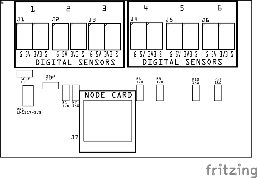
Assembly and Component Placement
This section combines both the component specifications and the assembly instructions to ensure a smooth assembly process. Below is a comprehensive list of components, their placement on the PCB, and orientation details to assist you during assembly.
High-Level Steps for Assembly:
- PCB for the card can be ordered from any PCB fabricator using these Gerber Files.
- Clean PCB with alcohol to remove residue. See Cleaning_PCB for details.
- See also: Soldering Tips
- PCB Components - listing of components used for PCB assembly
- PCB Parts - listing of parts used for PCB assembly
![]()
![]()
| Component Identifier | Count | Type | Value | Package | Purpose | Orientation |
|---|---|---|---|---|---|---|
| Capacitors | ||||||
| C1 | 1 | Ceramic Capacitor | 10uF | 1206 SMD | Filters high-frequency noise from input to 3V3 voltage regulator | None |
| C2 | 1 | Ceramic Capacitor | 22uF | 1206 SMD | Filters high-frequency noise from 3V3 voltage regulator output | None |
| Connectors | ||||||
| J1-J6 | 6 | JST XH Socket or 2-Position Spring Terminal Connector | 2P, 2.54mm | PTH, vertical or horizontal | Connectors to sensors | |
| J7 | 1 | RJ45 Socket | 8P8C | PTH | Network cable (CAT5/6) connection from Node Card | |
| Resistors | ||||||
| R1-R6 | 6 | Resistor | 100kΩ | 1206 SMD | Sets the op-amp gain for sensor resistances from ~1 kΩ to 1 MΩ, producing a 0–3.3 V output suitable for ESP32 ADC input. | |
| Regulator | ||||||
| VR1 | 1 | Voltage Regulator | LM1117-3V3 IC | SMD | 3.3 VDC regulator for Sensors | |
| Sensors | ||||||
| Potentiometer | 0-6 | n/a | 0 Ω–100 kΩ | n/a1 | controller. e.g. user selection detected to set room light level | |
| LDR | 0-6 | CDS Photoresistor | 0 Ω–100 kΩ | n/a2 | measure light. e.g. whether room lights are on/off | |
| FSR | 0-6 | Passive, resistive | 0-200g | Thin File Pressure Sensor3 | Force detection. e.g. determine whether car is present, or is loaded. User touched panel. |
- Potentiometer example; RV24YN20S shaft, 0-100kΩ
- Photoresistor example; GL5528 (Light ~10–20 kΩ, Dark >500 kΩ)
- FSR (Force Sensitive Resistor) example; 0-200g Thin Film Pressure Sensor Flexible Force Sensitive Resistance-type Sensor
Tools Required
Safety Precautions
- See Safety Precautions.
| Designator (value) | Component | Required? | Orientation |
|---|---|---|---|
| R1-R6 | 100kΩ, 1206 SMD | Required (one per sensor) | None |
| U1 | LM358 Op Amp | Required (one per sensor) | IC dimple/dot position to PCB top edge |
| J1-J6 | JST XH Socket, Terminal Connector | Required (one per sensor) | Position connection outward |
| J7 | RJ45 Socket | Required | Fits only one way |
Testing and Verification
Visual Inspection
- Initial Check: Examine the board for any obvious issues like missing components, solder bridges, or components that are misaligned or not fully seated.
- Solder Joint Inspection: Use a magnifying glass or a microscope to inspect solder joints. Look for cold solder joints, insufficient or excessive solder, or any shorts between pads.
- Use an Digital Multimeter (DMM) to test for continuity between:
- RJ45 socket pin 1 and each sensor VDC pin
- RJ45 socket pin 2 and each sensor G pin
- RJ45 socket pins 3-8 and each sensor S pin
Functional Testing
Troubleshooting
- See I2C Trouble Shooting.
Appendences
PCB Specifications
Specifications for the Resistive Sensor Breakout Board include:
| Characteristic | Value |
|---|---|
| Max Sensors (per breakout board) | 6 |
| Max Breakout Boards (per Node Card) | 1 |
| Digital Input | 3V3 |
| Digital Output | 3V3 |
| Dimension | 50mm x 72mm |
How It Works
The Digital Sensor Breakout Board connects directly to the LCC Fusion Node Card and provides six general-purpose Digital Sensor lines. It supports both digital inputs (such as sensors, switches, or buttons) and digital outputs (such as indicator LEDs, relays, or logic triggers), making it a flexible solution for layout interaction and automation.
Direct GPIO Connection
Each of the six I/O lines is connected through a 3-pin header labeled:
- V (3.3 V power)
- S (Signal)
- G (Ground)
The S pin of each header is connected directly to one of the Node Card’s GPIOs. These GPIOs are fully configurable in firmware as either inputs or outputs, depending on the application.
Input Mode
When configured as an input, the I/O line can accept logic-level signals from external devices such as:
- Capacitive touch sensors
- Hall effect sensors
- Mechanical switches
- Digital IR sensors
The firmware provides options for:
- Enabling internal pull-ups
- Setting debounce timing
- Detecting rising, falling, or both edges
- Triggering LCC Events when a state change is detected
Each input line includes a built-in 1 kΩ series resistor for protection against shorts or voltage mismatch, ensuring safe connection even in mixed-use environments.
Output Mode
When configured as an output, the Node firmware can drive the I/O lines to:
- Light up panel LEDs or route indicators
- Activate low-power relays or MOSFET gates
- Send logic signals to other modules or control devices
GPIO output states can be controlled directly by:
- Node-local logic (such as turnout or signal states)
- Incoming LCC Events from the CAN network
This allows the board to participate in coordinated actions across the layout, whether locally triggered or remotely controlled.
Simple Integration and Expansion
The board connects to the Node Card through a single RJ45 cable, carrying:
- GND and 3.3 V power
- Six signal lines (GPIOs)
It requires no hub or I²C interface and is ideal for direct plug-in applications where small, distributed control or sensing is needed. For larger-scale Digital Sensor needs, additional I²C-based boards can be added via the Node Bus Hub.
Connections
The purpose of the Resistive Sensor Breakout Board and its connectors is to facilitate quick and easy connections between the Node Card and resistive sensors.
| Component Designator | Connector Label | Connector Type | Connection Number | Description |
|---|---|---|---|---|
| J1 - J6 | SENSORS 1-6 | 3-pin JST XH, Spring Terminal | S, VDC, G | Signal, 3.3V, and GND connections to each sensor |
| J7 | NODE CARD | RJ45 Socket | 3v3, GND, S, S, S, S, S, S | Power and sensor connection with Node Card I/O connector (RJ45 socket) |