Use Cases: PCB Design & Assembly , Node Cluster Setup , Device Control , Automation Deployment
I/O Card Assembly Guide
Table of contents
Introduction
See the How to Use Assembly Guides for detailed instructions.
In conjunction with the LCC Fusion LCC Fusion Node Card and a Node Bus Hub, the I/O Card provides input and output control for up to 16 separate devices. Typically when used for input in an LCC Node arrangement, this card can be attached to input devices (buttons, sensors, etc.) to produce on/off event IDs. These IDs are subsequently consumed by the LCC Node, which then employs either this card for output, or the Output Card to accurately control the functioning states of the attached devices.
flowchart LR;
subgraph layout ["Train Layout"];
  direction LR;
  can["CAN Network"];
  can2["CAN Network"];
  nodecard[["Node Card"]];
  nodecard2["Node Card"];
  c[["I/O Card (16x)"]];
  c2[["I/O Card (16x)"]];
  bb[[I/O Breakout Board]];
  out(("Output Device (16x)"));
  in(("Input Device (16x)"));
  bb2[["I/O Breakout Baord"]];

  can --> |"LCC Event<br/>(on/off)"| nodecard;
  nodecard -->|"GPIO Input <br/> (High/Low)"| c;
  c --> |"Digital Output<br/>(high/low)"| bb;
  bb --> |"Digital Output <br/> (high/low)"| out;

  in --> |"Digital Input <br/> (high/low)"| bb2;
  bb2 --> |"GPIO Input <br/>(high/low)"| c2;
  c2 --> |"Digital Input <br/> (high/low)"| nodecard2;
  nodecard2 --> |"LCC Event<br/>(on/off)"| can2;
end;
classDef lSalmonStyle fill:#FFA07A,stroke:#333,stroke-width:2px,font-size:24px;
class c,c2 lSalmonStyle;
classDef lightGrayStyle fill:#d3d3d3,stroke:#333,stroke-width:2px,font-size:24px;
class layout lightGrayStyle;
- jumper_caps - not defined
- lcc_event_id - not defined
- lcc_fusion_io_cards - not defined
- lcc_fusion_node_bus - not defined
- lcc_fusion_node_card - not defined
- output_cards - not defined
For other terms, please refer to the full Terminology Guide.
Assembly and Component Placement
This section combines both the component specifications and the assembly instructions to ensure a smooth assembly process. Below is a comprehensive list of components, their placement on the PCB, and orientation details to assist you during assembly.
High-Level Steps for Assembly:
- PCB for the card can be ordered from any PCB fabricator using these Gerber Files.
- Clean PCB with alcohol to remove residue. See Cleaning_PCB for details.
- See also: Soldering Tips
- PCB Components - listing of components used for PCB assembly
- PCB Parts - listing of parts used for PCB assembly
Below is a list of the PCB components used for this card (see diagram before reference):
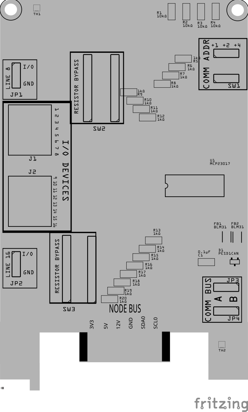
| Component Identifier | Count | Type | Value | Package | Purpose | Orientation |
|---|---|---|---|---|---|---|
| Capacitors | ||||||
| C1 | 1 | Capacitor-Ceramic | 0.1uF, 50 V | 1206 X7R | Decoupling capacitor for IC protection. | None |
| Diodes | ||||||
| D1 | 1 | ESD Diode | PESD1CAN | SOT-23 SMD | I2C data bus electrostatic discharge (ESD) protection. | Fits only one way |
| Filters & Noise Suppression | ||||||
| FB1, FB2 | 2 | Ferrite Bead | BLM31PG121SN1L | 1206 SMD | I2C network bus data line noise suppression. | None |
| Connectors | ||||||
| J1, J2 | 2 | RJ45 Socket | 8P8C | N/A | Network cable (CAT5/6) connection to I/O devices. | Fits only one way |
| Resistors | ||||||
| R5 - R23 | 19 | Resistor | 10kΩ | 1206 SMD | Used to limit current to the I/O devices. Required when limiting output current. Optionally bypassed by setting the corresponding DIP switch (SW2, SW3) to ON. Modify the resistor value to match the requirements of the I/O device. For LEDs, see Choosing the Right Resistor for LEDs. | None |
| R1 - R4 | 4 | Resistor | 10kΩ | 1206 SMD | Used to limit current to SW1 and MCP23017 for I2C address. | None |
| Selectors & Indicators | ||||||
| JP1, JP2 | 2 | Male Header | 3P, 0.1” spacing | N/A | Used for LINES 8 & 16 selection for either GND or I/O. Set to GND when I/O devices require this card to provide the circuit’s GND connection. | None |
| JP3, JP4 | 2 | Male Header | 3P, 0.1” spacing | N/A | Used for COMM BUS selection (I2C hardware bus) for either BUS A or BUS B. Must match the configuration within the LCC Node (CDI). | None |
| SH1, SH2, SH3, SH4 | 4 | Jumper Caps | 2.54mm | N/A | Used with I2C Bus and LINE 8/16 selections. Recommend tall caps for ease of use. | None |
| SW1 | 1 | DIP / Slide Switch | 3P, 2.54mm | N/A | Used for COMM ADDR selection (I2C address offset, 0-7). Up to 8 cards can be installed per I2C bus. Must match the LCC Node configuration (CDI). | Position so switch so ON is towards PCB top edge |
| SW2, SW3 | 2 | DIP / Slide Switch | 8P, 2.54mm | N/A | Used to enable/disable limiting resistors for each I/O line. Required to bypass current-limiting resistors (R5-R23). | Position so switch so ON is towards PCB top edge |
| ICs | ||||||
| U1 | 1 | IC | MCP23017 | SSOP28 | I/O expander using I2C serial interface to control 16 GPIO pins. | Position IC’s dent towards PCB right edge |
Tools Required
Safety Precautions
- See Safety Precautions.
Testing and Verification
Configure the card:
- Select the I2C bus (COMM BUS) by positioning (2) Jumper Caps on either BUS A or BUS B male header pins (JP1, JP2)
- Select the I2C address (COMM ADDR) switch (SW1) by slide each of the 3 switches to either the ON or OFF position. Setting a switch to ON increments the address by 1, 2, or 4 for an address range of 0 to 7. Up to 8 devices can then be configured for BUS A and 8 for BUS B.
- Select the output voltage by positioning a Jump Cap on (1) pair of VOLTAGE male header pins (JP5)
- Select the function of Line 16 as an output line or as a ground (GND) connection by positioning a Jumper Cap on (1) pair of LINE 8 and LINE 16 male header pins (JP3, JP4).
The following test and verifications of the card should be performed after a through inspection of the card’s soldering. Check all of the PTH component pins and SMD pads. Make sure there are no solder bridges between pins and pads.
Visual Inspection
-
Initial Check: Examine the board for any obvious issues like missing components, solder bridges, or components that are misaligned or not fully seated.
-
Solder Joint Inspection: Use a magnifying glass or a microscope to inspect solder joints. Look for cold solder joints, insufficient or excessive solder, or any shorts between pads.
-
Component Orientation: the IC’s are correctly oriented according to the PCB silkscreen or schematic.
Connectivity Testing
Power-Up Tests
- Assembly a tested Power Module to the LCC Fusion Node Card.
- Apply Power to the Power Module and verify the following:
- Check for Hot Components: Feel for components that are overheating, which could indicate a problem like a short circuit or incorrect component.
Functional Testing
I2C Verification
Line Verification
After validating the LCC Fusion Node Card can connect with the I/O Card, test each of the I/O lines as follows:
- Connect an network cable (CAT5/6) to RJ45 connector. Use the other end of the cable with a breakout board, or exposed wires to connect to devices for testing.
- Configure each line of the card for output using an LCC CDI Configuration Tool
- Attach an LED anode to each line. Attach the LED cathode to common (GND) used by the LCC Fusion Node Card.
- Set the current limiting DIP switches to ON
-
Test using LCC events:
-
Send the configured on/off LCC Event ID’s for each output line
-
Validate that LED(s) turn on/off
-
If some of the lines work and some don’t, it probably a soldering connection for the bad line
-
If none of the lines work correctly, check the connections for the voltage settings
-
-
Troubleshooting
- See I2C Trouble Shooting.
Appendences
Specifications
Specifications for the card include:
| Characteristic | Value |
|---|---|
| Output | 5V |
| Max Output Lines | 161 |
| Max Output Per Line (based on MCP23017 IC) | 25 mA1 |
| Maximum Number of Cards per LCC Fusion Node Cluster | 162 |
- For 12 V or higher output current, use the Output Card.
- The LCC Fusion Node Cluster can support up to 16 cards, distributed across two I2C hardware buses, with a maximum of 8 cards per bus.
- Note: total includes all cards using the I2C address range of
0x20(MCP23017 IC).
- Note: total includes all cards using the I2C address range of
- GND, 5V, 12 V (optional), SLA0/SDA0, and SDA1/SCL1 (optional)
How It Works
The following outlines the operational flow for the I/O Card, which implements an MCP23017 port expander connected to RJ45 sockets with current-limiting resistors that can be optionally set via slide switches:
The firmware of the LCC Fusion Node Card interfaces with the I/O Card’s MCP23017 port expander using I2C communication, following the bus and address details specified in the card’s CDI I2C section.
Output Operation:
- When an LCC Event is triggered, the LCC Fusion Node Card firmware sends an I2C command to the I/O Card, instructing the MCP23017 to set the specified port state (HIGH or LOW).
- The port expander adjusts the corresponding I/O line, setting it to either 5 V (HIGH) or GND (LOW), as instructed by the I2C command.
- The selector for LINE 8 and LINE 16 can be set to either
I/OorGNDto indicate the function of the line. When set toGNDthe line will connect the I/O device to the LCC Fusion Node BusGNDconnection. This is useful when the I/O device does not have access to this same GND connection (ground plane).
Note: For output functionality, devices like LEDs or relays should be connected to the I/O lines. These devices must share a common ground with the LCC Fusion Node Card through either Line 16 or the Accessory Bus.
Input Operation:
- The firmware configures the MCP23017 port expander with internal pull-up resistors (set to 3.3 V). When an input device (such as a switch) pulls an input line to LOW (GND), the corresponding GPIO line of the port expander is pulled to LOW.
- When the LCC Node firmware detects a GPIO state change to LOW, it generates an LCC Event to indicate the ON state. When the input device resets (e.g., the button is released), the GPIO line returns to HIGH, and the firmware generates an LCC Event for the OFF state.
Protection
The I/O Card provides input / output control of devices. The following is an overview of each protection component integrated into the I/O Card and its role:
| Protected Component | Protection Component | Function | Specifications | Location |
|---|---|---|---|---|
| MCP23017 IC | Decoupling Capacitors | Filters out high-frequency noise and transient voltage spikes from the power supply, ensuring stable voltage to MCP23017 IC. | Values: 0.1 µF ceramic | Across Vcc and GND near IC. |
| I2C Lines | Ferrite Bead BLM31PG121SN1L | Provides high-frequency noise suppression on the I2C lines. | Impedance: 120 ohms at 100 MHz | In series with the SDA and SCL lines of the I2C bus |
| I2C Lines | ESD Protection Diode PESD1CAN | Protects the I2C lines from electrostatic discharge and voltage spikes. | Reverse Stand-off Voltage (Vr): 24 V Clamping Voltage (Vc): 40 V |
Across the SDA and SCL lines to GND |
| I/O Lines | Current Limiting | Current limiting to protect I/O devices (i.e. LEDs) | Impedance: 1kΩ | In series with I/O lines, selectable via slide switch |
References
Overvoltage Protection