Node Analog Sensor Breakout Board Assembly Guide
Table of contents
Table of contents
Introduction
The Node Analog Sensor Breakout Board is designed to connect up to sixteen analog sensors to the LCC Fusion Node Card. It supports both 2-wire resistive sensors—such as photoresistors (LDRs), force-sensitive resistors (FSRs), and potentiometers—and 3-wire voltage-output sensors, such as infrared reflectance sensors, touch modules, and Hall effect devices.
The board includes two sensor input groups:
- 2-WIRE RESISTIVE SENSORS (CH1–CH8): Connected through an inverting op-amp circuit (LM358) and routed to MUX A
- 3-WIRE SENSORS (CH9–CH16): Connected directly to MUX B without amplification
Each multiplexer shares the same address lines but is independently enabled, allowing the Node Card to read any of the sixteen sensor inputs using a single ADC channel.
The Node firmware selects the appropriate MUX based on configuration, sets the address lines, and reads the sensor values through the shared ADC. Each input can be assigned a user-defined threshold. When a threshold is crossed, the firmware generates an LCC Event that can be used to trigger layout actions such as lighting control, animations, or other sensor-driven responses.
With onboard signal conditioning, modular expansion, and support for both resistive and voltage-output sensors, the Node Analog Input Breakout Board provides a flexible and reliable way to bring real-world sensing into your LCC network.
flowchart LR;
can["CAN Network"];
subgraph layout ["Train Layout"];
  direction LR;
  sensor1(("2-Wire Analog Sensors (8x)"));
  sensor2(("3-Wire Analog Sensors (8x)"));
  nodecard[[Node Card]];
  bb[["Node Analog Sensor<br>Breakout Board"]];


	sensor1 -->|"resistance<br>(0-3.3v)"| bb;
	sensor2 -->|"voltage<br>(0-3.3v)"|bb;
 	bb -.-> |"voltage<br>(0-3.3v)"| nodecard;
  nodecard -.->|"LCC Event <br/>car load (yes/no)"| can;
  nodecard -.->|"LCC Event <br/>lighting (on/off)"| can;
end;
classDef lSalmonStyle fill:#FFA07A,stroke:#333,stroke-width:2px,font-size:20px;
class bb lSalmonStyle;
classDef lightGrayStyle fill:#d3d3d3,stroke:#333,stroke-width:2px,font-size:24px;
class layout lightGrayStyle;
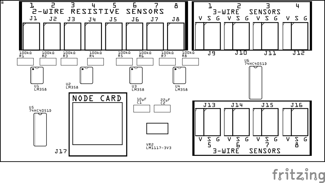
Assembly and Component Placement
This section combines both the component specifications and the assembly instructions to ensure a smooth assembly process. Below is a comprehensive list of components, their placement on the PCB, and orientation details to assist you during assembly.
High-Level Steps for Assembly:
- PCB for the card can be ordered from any PCB fabricator using these Gerber Files.
- Clean PCB with alcohol to remove residue. See Cleaning_PCB for details.
- See also: Soldering Tips
- PCB Components - listing of components used for PCB assembly
- PCB Parts - listing of parts used for PCB assembly
![]()
![]()
| Component Identifier | Count | Type | Value | Package | Purpose | Orientation |
|---|---|---|---|---|---|---|
| Capacitors | ||||||
| C1 | 1 | Ceramic Capacitor | 10uF | 1206 SMD | Filters high-frequency noise from input to 3V3 voltage regulator | None |
| C2 | 1 | Ceramic Capacitor | 22uF | 1206 SMD | Filters high-frequency noise from 3V3 voltage regulator output | None |
| Connectors | ||||||
| J1-J8 | 8 | JST XH Socket or 2-Position Spring Terminal Connector | 2P, 2.54mm | PTH, vertical or horizontal | Connectors to sensors | Position connection outward |
| J9-J16 | 8 | JST XH Socket or 3-Position Spring Terminal Connector | 23, 2.54mm | PTH, vertical or horizontal | Connectors to sensors | Position connection outward |
| J17 | 1 | RJ45 Socket | 8P8C | PTH | Network cable (CAT5/6) connection from Node Card | Fits only one way |
| Resistors | ||||||
| R1-R8 | 8 | Resistor | 100kΩ | 1206 SMD | Sets the op-amp gain for sensor resistances from ~1 kΩ to 1 MΩ, producing a 0–3.3 V output suitable for ESP32 ADC input. | None |
| IC’s | ||||||
| U1-U4 | 4 | Dual Op Amp, LM358DR | n/a | SOP-8, SMD | Amplifies voltage across the sensor to produce a stable 0–3.3 V signal for the ESP32 ADC, based on sensor resistance and gain resistor. Each supports 2x sensors. | IC dimple/dot positioned to PCB top edge |
| U5, U6 | 2 | MUX, 74HC4051D | n/a | SO-16 | Allows the Node Card to read multiple (8x) sensor signals using a single ADC input by selecting one sensor line at a time. One is used for 2-wire sensors, 2nd is used for 3-wire sensors. | IC indent positioned to PCB top edge |
| Regulators | ||||||
| VR1 | 1 | Voltage Regulator | LM1117-3V3 IC | SMD | 3.3 VDC regulator for Sensors | Fits only one way |
| Sensors | ||||||
| Potentiometer | 0-6 | n/a | 0 Ω–100 kΩ | n/a1 | controller. e.g. user selection detected to set room light level | |
| LDR | 0-6 | CDS Photoresistor | 0 Ω–100 kΩ | n/a2 | measure light. e.g. whether room lights are on/off | |
| FSR | 0-6 | Passive, resistive | 0-200g | Thin File Pressure Sensor3 | Force detection. e.g. determine whether car is present, or is loaded. User touched panel. |
- Potentiometer example; RV24YN20S shaft, 0-100kΩ
- Photoresistor example; GL5528 (Light ~10–20 kΩ, Dark >500 kΩ)
- FSR (Force Sensitive Resistor) example; 0-200g Thin Film Pressure Sensor Flexible Force Sensitive Resistance-type Sensor
Tools Required
Safety Precautions
- See Safety Precautions.
Testing and Verification
Visual Inspection
- Initial Check: Examine the board for any obvious issues like missing components, solder bridges, or components that are misaligned or not fully seated.
- Solder Joint Inspection: Use a magnifying glass or a microscope to inspect solder joints. Look for cold solder joints, insufficient or excessive solder, or any shorts between pads.
- Use an Digital Multimeter (DMM) to test for continuity between:
- RJ45 socket pin 1 and each sensor VDC pin
- RJ45 socket pin 2 and each sensor G pin
- RJ45 socket pins 3-8 and each sensor S pin
Functional Testing
Troubleshooting
- See I2C Trouble Shooting.
Appendences
PCB Specifications
Specifications for the Resistive Sensor Breakout Board include:
| Characteristic | Value |
|---|---|
| Max Sensors (per breakout board) | 16 |
| Max Breakout Boards (per Node Card) | 1 |
| 2-Wire Resistive Sensor | 0Ω - 100kΩ |
| 3-Wire Voltage | 3V |
| Dimension | 50mm x 100mm |
How It Works
The Node Analog Sensor Breakout Board allows up to sixteen analog sensors to be read by a single LCC Fusion Node Card using two multiplexers and a shared ADC input. The board supports both 2-wire resistive sensors and 3-wire voltage-output sensors, each with its own optimized signal path.
RESISTIVE SENSORS (CH1–CH8)
Resistive sensors—such as photoresistors (LDRs), force-sensitive resistors (FSRs), and potentiometers—connect to the board using 2-pin headers labeled V (Voltage) and S (Signal).
Each sensor forms part of an active sensing circuit using an inverting amplifier configuration built around the LM358 op-amp, with a 100 kΩ feedback resistor. This setup eliminates the need for a traditional voltage divider and provides a clean analog voltage output that varies based on the sensor’s resistance.
The op-amp outputs are routed to the inputs of MUX A, an 8-channel analog multiplexer. The Node Card uses three shared address lines (MUX_A, MUX_B, MUX_C) to select the active sensor channel. The firmware enables MUX A when accessing channels 1–8.
3-WIRE INPUTS (CH9–CH16)
Voltage-output sensors—such as HTTM capacitive touch sensors, TCRT5000 IR sensors, A3144 Hall effect sensors, and analog tilt or vibration modules—connect using 3-pin headers labeled V (3.3V), S (Signal), and G (Ground).
These sensors provide a direct voltage signal on the S line. That signal is routed directly to MUX B, bypassing amplification. MUX B is also controlled by the same address lines (A–C), and is enabled by the firmware when accessing lines 9–16.
Firmware-Based BUS Control
Rather than using a physical jumper or switch, the Node firmware determines which MUX to enable—MUX A for channels 1–8, and MUX B for channels 9–16—based on the user’s configuration. The firmware sets the correct address (0–7), enables the appropriate MUX, and reads the resulting signal through the ADC.
This design allows both sensor types to be supported on the same board simultaneously, using only a single RJ45 connection to the Node Card. It simplifies installation, keeps hardware flexible, and maintains full compatibility with the LCC Fusion network structure and configuration model.
Connections
The purpose of the Resistive Sensor Breakout Board and its connectors is to facilitate quick and easy connections between the Node Card and resistive sensors.
| Component Designator | Connector Label | Connector Type | Connection Number | Description |
|---|---|---|---|---|
| J1 - J8 | 2-WIRE RESISTIVE SENSORS 1-8 | 2-pin JST XH, Spring Terminal | n/a | For 2-wire resistive sensors, connect across VDC and S; G is not required but can remain connected |
| J9 - J16 | 3-WIRE SENSORS 1-8 | 3-pin JST XH, Spring Terminal | VDC, S, G | For 3-wire voltage-output sensors, use S (Signal), VDC (Power), and G (Ground) |
| J17 | NODE CARD | RJ45 Socket | GND, 5V, ADC, ENA, ENB, MUXA, MUXB, MUXC | Power and sensor connection with Node Card I/O connector (RJ45 socket) |