Node Bus Hub Repeater Assembly Guide
Table of contents
Table of contents
Introduction
See the How to Use Assembly Guides for detailed instructions.
The Node Bus Hub Repeater is an optional expansion board for the LCC Fusion Project designed to improve I²C signal integrity across long Node Bus cable runs. It buffers both I²C Bus A and Bus B using onboard PCA9515A ICs, creating isolated segments that reduce capacitive loading and restore clean signal edges.
To ensure proper operation of each I²C segment, the board also includes automatic pull-up detection and activation for both SDA and SCL lines. This dynamic system engages pull-up resistors only when needed, preventing redundant loading across the Node Bus.
Use this board when connecting Node Bus Hubs with long network cables (typically over 5 meters) or in electrically noisy environments to maintain reliable communication between I/O cards and Node Cards.
Note: This board only conditions the I²C communication lines. All other Node Bus lines—including power (3.3 V, 5 V, 12 V, GND) and the CAN bus—pass through the repeater board unbuffered and unmodified.
flowchart LR;
can["CAN Network"];
hub[["Node Bus Hub"]];
hub2[["Node Bus Hub"]];
repeater[["Node Bus<br> Hub Repeater"]];
n[["Node Card"]];
pc[["Power-CAN Card"]];
iocards[["I/O Cards"]];
iocards2[["I/O Cards"]];

subgraph layout ["Train Layout"];
direction LR;
can --> n --> hub;
can --> pc;
pc --> hub;
hub --> iocards --> devices((Devices));
hub --> |"Long Network Cable<br>(>5m)"| repeater;
repeater --> hub2;
hub2 --> iocards2 --> devices2((Devices));
end

classDef lSalmonStyle fill:#FFA07A,stroke:#333,stroke-width:2px,font-size:24px;
class repeater lSalmonStyle;
classDef lBlueStyle fill:lightBlue,stroke:#333,stroke-width:2px,font-size:24px;
class hub,hub2 lBlueStyle;
classDef lightGrayStyle fill:#d3d3d3,stroke:#333,stroke-width:2px,font-size:24px;
class layout lightGrayStyle;
![]()
Assembly and Component Placement
This section combines both the component specifications and the assembly instructions to ensure a smooth assembly process. Below is a comprehensive list of components, their placement on the PCB, and orientation details to assist you during assembly.
High-Level Steps for Assembly:
- PCB for the card can be ordered from any PCB fabricator using these Gerber Files.
- Clean PCB with alcohol to remove residue. See Cleaning_PCB for details.
- See also: Soldering Tips
- PCB Components - listing of components used for PCB assembly
-
PCB Parts - listing of parts used for PCB assembly
- 6x-Node Bus Hub (use with up to 6 cards, with expansion capabilities with more 6x Node Bus Hubs, typically used in a central location). This implementation of the Node Bus Hub also provides:
- Selection for adding I2C pull-up for long I2C serial connections to improve signal quality.
- Network cable connections (RJ45) to allow expansion to additional Node Bus Hubs.
- Connectors (female pin headers) to allow expansion to additional Node Bus Hubs.
- LED indicators for I2C data transmission for BUS A and BUS B. A transistor is used to trigger the LEDs to sense data transmissions from the I2C TX (transmission) line going HIGH during data transmissions.
- 5V power supply connection (USB-C) for providing power when the expansion board is not being powered by a Primary LCC Fusion Node Card (with a Power Module).
- Depending on requirements, 1 to 6 connectors can be installed on either side.
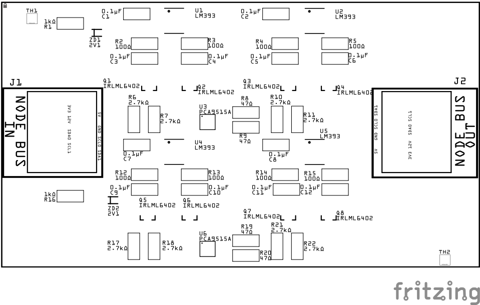
Below is a list of the PCB components used for the 6x Node Bus Hub (see diagram on right for reference):
![]()
![]()
| Component Identifier | Count | Type | Value | Package | Purpose | Orientation |
|---|---|---|---|---|---|---|
| Capacitors | ||||||
| C1–C4 | 4 | Capacitor-Ceramic | 0.1 µF | SMD 1206 | Power decoupling for LM393 and PCA9515A ICs | None |
| C5–C8 | 4 | Capacitor-Ceramic | 0.1 µF | SMD 1206 | RC low-pass filter for I²C voltage sensing | None |
| Diodes | ||||||
| ZD1, ZD2 | 2 | Zener Diode | 2.1 V | BZT52 | Reference voltage source for voltage comparators (one per I²C bus) | Cathode end has a white line and positioned towards PCB left edge |
| Transistors | ||||||
| Q1–Q8 | 8 | PNP Transistor | IRLML6402 | SOT-23 | Controls when 2.7 kΩ pull-ups are applied to I²C lines | Fits only one way |
| Resistors | ||||||
| R1, R16 | 2 | Resistor | 1 kΩ | SMD 1206 | Bias resistor feeding Zener diodes | None |
| R2–R5, R12-R15 | 8 | Resistor | 100 Ω | SMD 1206 | Forms part of the low-pass filter for SCL/SDA sensing (to -IN) | None |
| R6, R7, R10, R11, R17, R18, R21, R22 | 8 | Resistor | 2.7 kΩ | SMD 1206 | Pull-up resistor for I²C lines (enabled via PNP transistor) | None |
| R8, R9, R19, R20 | 4 | Resistor | 47 kΩ | SMD 1206 | Passive pull-up or signal conditioner between the PCA line and the base of the NPN | None |
| ICs | ||||||
| U1, U2, U4, U5 | 4 | IC – Comparator | LM393 | SOIC-8 | Detects voltage drop below 2.1 V on I²C lines to activate pull-ups | Pin 1 dimple toward top edge |
| U3, U6 | 2 | IC – I²C Repeater | PCA9515A | TSSOP-8 | Buffers I²C into isolated segments for longer, more reliable cabling | Pin 1 dimple toward top edge |
| Connectors | ||||||
| J1 | 1 | RJ45 Socket | 8P8C | - | Node Bus IN — connects to previous hub via CAT5/6 cable | Fits only one way |
| J2 | 1 | RJ45 Socket | 8P8C | - | Node Bus OUT — connects to next hub via CAT5/6 cable | Fits only one way |
Tools Required
The card only requires soldering three sets of PTH female pin headers. Required tools required are:
- soldering iron
- solder
- tacky putty (hold components while soldering)
See List of recommended tools for more details on these tools.
Safety Precautions
Testing and Verification
The following test and verifications of the card should be performed after a through inspection of the card’s soldering. Check all of the PTH component pins. Make sure there are no solder bridges between pins.
Visual Inspection
- Initial Check: Examine the board for any obvious issues like missing components, solder bridges, or components that are misaligned or not fully seated.
- Solder Joint Inspection: Use a magnifying glass or a microscope to inspect solder joints. Look for cold solder joints, insufficient or excessive solder, or any shorts between pads.
Power-Up Tests
Refer to the LCC Fusion Node Card for details on testing the LCC Fusion Node Bus Hub
Troubleshooting
- See I2C Trouble Shooting.
Appendences
PCB Specifications
Specifications for the Node Bus Hub include:
| Characteristic | Value |
|---|---|
| Input / Output | 3V3, 5V, 12 VDC |
| Max Input | 35 VDC |
| Hardware Communication Buses (I2C) | 2 |
| CAN (Controller Area Network) | 1 |
| DCC (Digital Command Control) | 1 |
| Expansion Board Connectors | 4 |
- Power connections for 3V3, 5V, 12 VDC.
- MAX current 1.7A (based on 24 mil trace width, 1oz)
- MAX connectors; 6 (6x Node Bus Hub), 2 (2x Node Bus Hub)
- Indicators (6x Node Bus Hub); 5V (red), I2C data transmit (GRN), I2C data receive (RED)
How It Works
The LCC Fusion Project’s Node Bus Hub is a versatile PCB designed to streamline the connection and management of multiple LCC (Layout Command Control) devices in a model railroad automation setup. Here’s a detailed overview of its features and functionality:
- Card Edge Connectors: The Node Bus Hub is equipped with up to 6x 805 card edge 2x6 connectors. These connectors provide parallel connections for multiple critical signals and power lines, including:
- 3.3 VDC
- 5 VDC
- 12 VDC
- CAN (Controller Area Network)
- Two I2C (Inter-Integrated Circuit) buses
- DCC (Digital Command Control)
-
RJ45 Sockets and Pin Headers: The PCB includes RJ45 sockets and pin headers that allow for easy interconnection of multiple hubs, enabling flexible expansion and connectivity between different parts of the layout.
-
LED Indicators: The hub features LED indicators for monitoring the I2C bus status. These LEDs provide visual feedback on SDA (Serial Data Line) transfer activity, helping users quickly identify any communication issues.
-
BSS138 Transistor: A BSS138 MOSFET transistor is integrated into the circuit, assisting with I2C bus communication and particularly with LED status indication. This component ensures reliable signal level shifting and smooth operation of the I2C buses.
-
USB-C Power Option: For testing purposes without a Power-CAN Card, the Node Bus Hub can be powered via a 5V USB-C connection. This feature includes a power indicator LED and reverse flow protection to prevent any potential damage from incorrect power flow.
- Communication Protection: To protect the communication lines, the Node Bus Hub utilizes PESD1CAN protection devices for both I2C buses and the CAN network. These components help safeguard the hub and connected devices from electrostatic discharge (ESD) and other transient voltage spikes.
Automatic I2C Pull-Up Conditioning
The LCC Fusion Node Bus Hub includes automatic I²C pull-up conditioning to ensure robust and reliable communication across connected devices. This feature dynamically enables pull-up resistors only when needed, based on real-time voltage monitoring of the SDA and SCL lines, reducing unnecessary bus loading while maintaining signal integrity.
Each hub monitors its local I²C segment independently using a dedicated circuit consisting of an LM393 comparator, Zener voltage reference, and a PNP transistor (e.g., IRLML6402). The result is a self-regulating bus that stays stable across variable distances and device counts.
- Voltage Monitoring
- The SDA and SCL lines are continuously monitored by the LM393 comparator.
- Voltage on each line is compared to a fixed reference (~2.4 V) provided by a Zener diode.
- If the idle voltage is below this threshold, it indicates no other active pull-up is present on the segment, and the comparator activates the local pull-ups.
- Dynamic Pull-Up Activation
- When triggered, the comparator output drives the base of a PNP transistor.
- This connects 3.3 V through a 2.7 kΩ resistor to the affected I²C line (SDA or SCL), restoring proper voltage and line strength.
- Low-Pass Filtering
- A low-pass RC filter on the comparator input prevents false triggering due to high-frequency noise or normal I²C traffic.
- This ensures that only true idle line degradation activates the pull-up.
- I²C Line Stability
- The circuit only engages pull-ups when no other hub is maintaining the bus.
- This avoids redundant pull-ups that would unnecessarily lower the effective resistance and load the I²C master.
- Dual-Bus Monitoring
- Both I²C Bus A and I²C Bus B are supported independently.
- Each bus has its own comparator, Zener diode, transistor, and pull-up resistors, ensuring reliable operation across both communication paths.
This automatic pull-up system allows every LCC Fusion Node Bus Hub — including the 1×, 2×, and 6× variants — to intelligently manage its I²C segment. The result is improved I²C reliability in complex, daisy-chained layouts with unknown segment lengths or numbers of devices, all without requiring manual configuration or solder jumpers.
Connections
The purpose of the Node Bus Hub and its connectors is to facilitate quick and easy connections between the LCC Fusion cards. For setups with requiring expansion, the Node Bus Hub provides connections to additional hubs.
![]()
| Component Designator | Connector Label | Connector Type | Connection Number | Description |
|---|---|---|---|---|
| J1, J2, J3, J4, J5, J6 | CARD-1 to CARD-6 | Card Edge Connector | 1 - 6 | Connection to LCC Fusion Cards |
| J7, J8, J11, J12 | NODE BUS | Female Header | n/a | Connection to another Node Bus Hub using pin headers |
| J9, J10 | NODE BUS | RJ45 Socket | N/A | Connection to another Node Bus Hub using a network cable |
PCB Protection
![]()
| Protected Component | Protection Component | Function | Specifications | Location |
|---|---|---|---|---|
| I2C Connection | PESD1CAN Diodes | Protect against ESD (Electrostatic Discharge) from the CAN network lines | Reverse Stand-off Voltage (Vr): 24 VDC Clamping Voltage (Vc): 40 VDC |
Across each I2C line (SDA, SCL) input line and GND |
| CAN Connection | PESD1CAN Diodes | Protect against ESD (Electrostatic Discharge) from the CAN network lines | Reverse Stand-off Voltage (Vr): 24 VDC Clamping Voltage (Vc): 40 VDC |
Across each CAN line (CAN-H, CAN-L) input line and GND |
| Power Supply (USB-C Option) | Reverse Flow Protection | Prevents damage from incorrect power flow direction. | Reverse polarity protection | USB-C power input |
| I2C Buses | 2.7k Ohm Pull-up Resistors | Stabilizes I2C communication by providing additional pull-up resistance. | 2.7k ohm resistors | Activated via jumper cap |