Output Card Assembly Guide
[TOC]
Introduction
See the How to Use Assembly Guides for detailed instructions.
The Output Card works in conjunction with the LCC Fusion Node Card and Node Bus Hub to provide control over up to 16 individual output devices. These devices can be actuated in response to LCC Events, allowing for automation and interaction within the layout. The Output Card interprets event IDs generated by sensor-based cards or other event sources, and then controls the corresponding output devices, providing a robust solution for managing lighting, motors, and more within your model train layout or other automated systems.
Through this design, the Output Card offers precise ON/OFF control for each connected device, enabling seamless interaction between the layout’s automation logic and the physical components.
Key Features:
- Controls up to 16 Output Devices: The Output Card offers up to 16 output lines, allowing you to control a wide range of devices like LEDs, relays, motors, and more.
- Supports Configuring up to 16 Output Cards per LCC Node: Each LCC Node can support up to 16 Output Cards, providing extensive output control for large or complex layouts. This allows up to 256 individual outputs across a single node, giving users incredible flexibility for controlling multiple devices.
- Selectable 5V or 12 VDC Output: Each output can be configured to deliver either 5 VDC or 12 VDC, providing flexibility to control devices that require different voltage levels. This makes the Output Card compatible with a variety of low-voltage and higher-power devices.
- Flexible Voltage Options: Output can be configured for either 5V or 12 VDC devices, providing versatility for different types of equipment.
- Configurable Resistor Options: Choose to use integrated current-limiting resistors or external resistors, depending on the power requirements of your devices.
- Lines 8 & 16 Flexibility: The 8th and 16th output line can be configured for standard output control or alternatively used as a ground (GND) connection, adding extra wiring flexibility to the design.
Typical Use Cases:
The Output Card can control a variety of devices for model train layouts, industrial automation, or hobbyist projects, offering flexibility and reliability.
Example Devices:
- LEDs: Control layout signals, indicators, or lighting effects using simple ON/OFF control.
- Relays: Switch larger loads such as lights, track power, or other high-power devices.
- DC Motors: Drive small motors for moving elements, such as turntables or gates.
- Buzzers: Trigger alarms or audio indicators in response to layout events.
- Solenoids/Electromagnets: Control solenoid-based mechanisms like point motors for turnouts or electromagnets for uncoupling systems.
- Fans: Activate ventilation systems or cooling fans for system components or scenery effects.
System Overview:
The Output Card is part of the LCC Node ecosystem and is typically controlled by the LCC Fusion Node Card, which processes LCC Events. When a sensor-based card detects an event (such as a train passing, a switch being thrown, or a button being pressed), it generates an event ID. The LCC Node consumes this ID and sends the appropriate signal to the Output Card, which then toggles the corresponding output device ON or OFF based on the event logic.
For example:
- A track sensor detects a train approaching a signal, generating an LCC event.
- The Node Card interprets the event and sends a command to the Output Card.
- The Output Card then turns on an LED to signal “stop” or activates a relay to power a motor or solenoid.
  flowchart LR
  can["CAN Network"];
  subgraph layout ["Train Layout"];
direction LR;
can --> |"LCC Event<br/>(on/off)"| n["Node Card"];
n -->|"GPIO Signal <br/> (high/low)"| c["Output Card (16x)"];
c --> |"Power <br/> (5 VDC/12 on/off)"| bb["Digital I/O  Breakout Board"];
bb -->|"Power <br/> (5 VDC/12 on/off)"| device(("Devices (16x)"));
c --> |"Power <br/> (5 VDC on/off)"| relay["Relay <br/> Breakout Board"];
relay --> |"Power <br/> (5 VDC on/off)"| devices(("Devices (8x)"));
  end
  classDef lSalmonStyle fill:#FFA07A,stroke:#333,stroke-width:2px,font-size:24px;
  class c lSalmonStyle;
  classDef lightGrayStyle fill:#d3d3d3,stroke:#333,stroke-width:2px,font-size:24px;
  class layout lightGrayStyle;
Hardware Configuration Options:
The Output Card includes several configurable options, allowing for flexibility in different scenarios:
- Communication Address: The card supports two I2C buses (bus 0 or 1) and offers address offsets from 0 to 7, enabling multiple cards to be used within the same node.
- Voltage Selection: The output voltage can be configured for either 5V or 12 VDC devices, making it compatible with a wide range of components.
- Resistor Configuration: Choose whether to use built-in current-limiting resistors for each output or to use external resistors, depending on the device’s power needs.
- Line 16 Configuration: Line 16 can either be used as a standard output line or as a ground connection (GND), providing additional flexibility for powering devices.
Assembly and Component Placement
This section combines both the component specifications and the assembly instructions to ensure a smooth assembly process. Below is a comprehensive list of components, their placement on the PCB, and orientation details to assist you during assembly.
High-Level Steps for Assembly:
- PCB for the card can be ordered from any PCB fabricator using these Gerber Files.
- Clean PCB with alcohol to remove residue. See Cleaning_PCB for details.
- See also: Soldering Tips
- PCB Components - listing of components used for PCB assembly
- PCB Parts - listing of parts used for PCB assembly
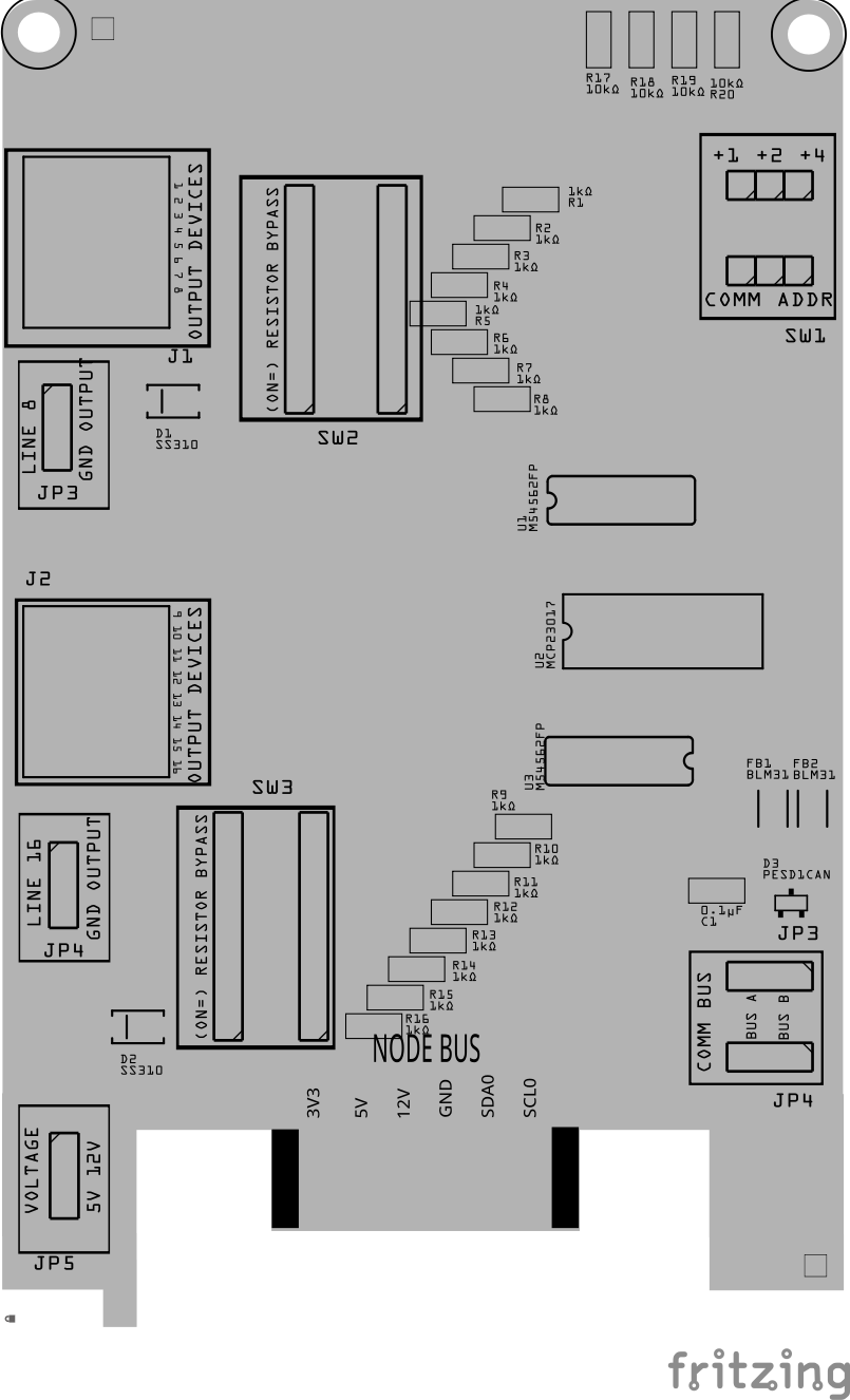
Below is a list of the PCB components used for this card (see diagram before reference):
![]()
![]()
| Component Identifier | Count | Type | Value | Package | Purpose | Orientation |
|---|---|---|---|---|---|---|
| Capacitors | ||||||
| C1, C2 | 2 | Capacitor-Ceramic | 0.1uF | 1206 X7R | Decoupling Capacitor for IC Protection | None |
| Diodes | ||||||
| D1, D2 | 2 | Diode-Schottky | SS310 | SMD | Circuit protection from reverse current from the lines | Cathode end has a white line and positioned towards PCB left edge |
| D3 | 1 | ESD Diode | PESD1CAN | SOT-23 SMD | I2C data bus electrostatic discharge (ESD) protection | Fits only one way |
| Filters & Noise Suppression | ||||||
| FB1, FB2 | 2 | Ferrite Bead | BLM31PG121SN1L | 1206 SMD | I2C Network Bus Data Line Noise Suppression | None |
| Connectors | ||||||
| J1, J2 | 2 | RJ45 Socket | 8P8C | PTH | Network cable (CAT5/6) connection to a breakout board or the Output’s I/O connector. | Fits only one way |
| Resistors | ||||||
| R1-R16 | 16 | Resistor | 1kΩ | 1206 SMD | Limits current to the output device. May be bypassed by setting the corresponding DIP switch (SW2, SW3) to ON. | None |
| R17-R19 | 3 | Resistor | 10kΩ | 1206 SMD | Limits current to SW1 and MCP23017 for I2C address configuration. | None |
| Selectors | ||||||
| JP1, JP2 | 2 | Male Header | 3P, 0.1” spacing | PTH | COMM BUS selection (I2C hardware bus) for BUS A or BUS B. Must match configuration in the LCC Node CDI setup. | None |
| JP3, JP4 | 1 | Male Header | 3P, 0.1” spacing | PTH | LINE 8 and LINE 16 selection to GND or Output. Set to GND when Output devices require this card to provide the GND connection. | None |
| JP5 | 1 | Male Header | 3P, 0.1” spacing | PTH | VOLTAGE selection for setting Vcc for output lines. Affects all output lines (e.g., 5V for LEDs, 12 VDC for relays). | None |
| SH1-SH5 | 5 | Jumper Caps | 2.54mm | N/A | Used with I2C Bus and Vcc selections. Tall caps are recommended for easy handling. | None |
| Switches | ||||||
| SW1 | 1 | DIP / Slide Switch | 3P, 2.54mm spacing | PTH | COMM ADDR selection (I2C address offset 0-7). Added to base address of MCP23017 (0x20). Configure for CDI setup. | Position so switch so ON is towards PCB top edge |
| SW2, SW3 | 2 | DIP / Slide Switch | 8P, 2.54mm spacing | PTH | Enable/disable current limiting resistors (R1-R16). Used to bypass the resistors for higher current outputs. | Position so switch so ON is towards PCB top edge |
| ICs | ||||||
| U1, U3 | 2 | Darlington Transistor | M54562FP | SOP20 | Amplifies low-current signals from MCP23017, driving high-current loads on output lines. | - IC U1 indent (pin 1) is positioned towards PCB left edge - IC U3 indent (pin 1) is positioned towards PCB right edge |
| U2 | 1 | I/O Expander | MCP23017 | SSOP28 | Expands I2C serial interface to control 16 GPIO pins, each connected to an output line. | IC indent (pin 1) is positioned towards PCB left edge |
| U4 | 1 | EEPROM | AT24C02 | SOIC-8 | Memory for card’s type and description | IC indent is positioned towards PCB right edge |
Tools Required
Safety Precautions
- See Safety Precautions.
Testing and Verification
Configure the card:
- Select the I2C bus (COMM BUS) by positioning (2) Jumper Caps on either BUS A or BUS B male header pins (JP1, JP2)
- Select the I2C address (COMM ADDR) switch (SW1) by slide each of the 3 switches to either the ON or OFF position. Setting a switch to ON increments the address by 1, 2, or 4 for an address range of 0 to 7. Up to 8 devices can then be configured for BUS A and 8 for BUS B.
- Select the output voltage by positioning a Jump Cap on (1) pair of VOLTAGE male header pins (JP5)
- Select the function of Line 16 as an output line or as a ground (GND) connection by positioning a Jumper Cap on (1) pair of LINE 8 and LINE 16 male header pins (JP3, JP4).
The following test and verifications of the card should be performed after a through inspection of the card’s soldering. Check all of the PTH component pins and SMD pads. Make sure there are no solder bridges between pins and pads.
Visual Inspection
-
Initial Check: Examine the board for any obvious issues like missing components, solder bridges, or components that are misaligned or not fully seated.
-
Solder Joint Inspection: Use a magnifying glass or a microscope to inspect solder joints. Look for cold solder joints, insufficient or excessive solder, or any shorts between pads.
-
Component Orientation: the IC’s are correctly oriented according to the PCB silkscreen or schematic.
Connectivity Testing
- Continuity Check: Use a multimeter in continuity mode to check for shorts between power rails and ground, and to ensure there are no open circuits in critical connections.
Power-Up Tests
- Assembly a tested Power Module to the LCC Fusion Node Card.
- Apply Power to the Power Module and verify the following:
- Check for Hot Components: Feel for components that are overheating, which could indicate a problem like a short circuit or incorrect component.
Functional Testing
I2C Verification
- Verify that the I2C connection between the LCC Fusion Node Card and the Output Card work. See Testing I2C Cards for details on how to test the I2C for a I2C enabled card.
Output Line Verification
After verifying that the LCC Fusion Node Card can communicate with the Output Card, test each output line as follows:
- Connect the network cable (CAT5/6)
Plug one end into the Output Card’s RJ45 port and the other into either:- a Card Monitor Board (recommended), or
- a breakout board / exposed leads for direct connection to test devices.
-
Configure each line for output
Use the LCC CDI Configuration Tool to assign the desired ON/OFF Event IDs and ensure each line is set for output mode. - Attach LEDs for visual testing
- Option 1: Plug the Card Monitor Board directly into the Output Card.
- Option 2: Manually connect each LED’s anode to a line and its cathode to the common GND used by the Node Card.
-
Set the Output Card’s VCC (typically 5 VDC or 12 VDC).
-
Set the current-limiting DIP switches to OFF when using the Card Monitor Board (it already includes 2.7 kΩ resistors). Enable them only when driving external devices directly.
- Test with LCC events
- Send the configured ON/OFF Event IDs for each output line.
- Observe LED activity: each line should switch ON/OFF as the events are received.
- If only some lines respond, recheck solder joints or DIP switch settings for those lines.
- If none respond, verify the voltage-select jumper and power connections.
Using Card Monitor Board for Testing Outputs
Connecting the Card Monitor Board to the Output Card allows you to quickly verify each output line visually.
Each LED on the monitor board corresponds to one output line (L1 – L8).
| Line(s) | What You Should See | How to Read It |
|---|---|---|
| L1 – L6 | Off (default) → On when the line is driven HIGH | Each LED lights when its line outputs voltage. Off = LOW / inactive. |
| L7 | Always On if the line is configured as VDC+ (power) Off (default) → On when driven HIGH (if used as I/O) |
Line 7 can either supply power to devices (steady ON) or act as a normal output line. |
| L8 | Selectable via JP1 Always Off if set to GND Off (default) → On when driven HIGH (if set to OUTPUT)** |
JP1 determines whether Line 8 serves as the board’s GND return or as an output line. Set to GND if your Output Card provides ground on L8; set to OUTPUT if the card uses L8 as a line. |
Notes:
- If your Output Card does not provide ground on L8, connect the Card Monitor Board’s J1 GND connector to the same power-supply ground as the Output Card.
- LEDs indicate digital line activity only — they show ON/OFF logic state, not current draw or load performance.
- LED brightness will vary slightly with output voltage (3.3 VDC → dim, 12 VDC → bright).
- A line stuck ON or OFF typically indicates a solder bridge, open trace, or mis-configured output.
Tip: For multi-line testing, configure a set of LCC events that toggle lines sequentially (L1 → L2 → L3 …). This makes it easy to confirm that all eight outputs respond correctly.
Using the Serial Menu for Testing Outputs
The LCC Fusion Serial Menu provides an alternative way to verify the Output Card lines without sending LCC Events. This method is ideal for quick bench testing after assembly or installation and can be used with LEDs or the Card Monitor Board.
Prerequisite: Ensure that a Node Card firmware build supporting the Serial Menu has been flashed to the Node Card.
Procedure
- Connect the Output Card to the Node Card using the Node Bus Hub
- Attach LEDs or the Card Monitor Board to the Output Card’s RJ45 connector.
- If using the Card Monitor Board, turn OFF any current-limiting DIP switches (it already includes 2.7 kΩ resistors).
- Open a Serial Monitor (YAT app, Bluetooth Serial Terminal app, or Arduino IDE) to the Node Card’s USB port and set the baud rate to 115200.
- Access the Serial Menu by typing the following commands sequentially in the serial monitor:
- Enter
M– opens the Main Menu - Enter
1– opens [1] Node Management - Enter
1– opens [1] Device Testing Management - Enter
5– selects [5] Simulate MCP Device Input
- Enter
- When prompted:
- Select the MCP device from the list hexadecimal address from discovered devices. Your Output Card’s address is
0x20 +the Output Card’s address offset. - Enter the pin number (0–15) you wish to drive HIGH
- Select the MCP device from the list hexadecimal address from discovered devices. Your Output Card’s address is
- Observe the LED (or Card Monitor Board line) corresponding to the selected pin turning ON. Repeat for other pins as needed.
Tip: This method is especially useful when performing Output Card diagnostics or verifying the I²C connection between the Node Card and Output Card before configuring LCC events.
Provisioning the Card
- See Provisioning a Card.
Troubleshooting
- See I2C Trouble Shooting.
Appendences
PCB Specifications
Specifications for the card include:
![]()
| Characteristic | Value |
|---|---|
| Output | 5 VDC, 12 VDC (selectable) |
| Max Output Line (based on M54562FP IC) | 500 mA |
| Max Output Lines | 16 |
| Max Number of Output Lines | 16 |
| Maximum Number of Cards (per LCC Fusion Node Cluster) | 161 |
- The LCC Fusion Node Cluster can support up to 16 cards, distributed across two I2C hardware buses, with a maximum of 8 cards per bus.
- Note: total includes all cards using the I2C address range of
0x20(MCP23017 IC).
- Note: total includes all cards using the I2C address range of
- GND, 5V, 12 VDC (optional), SLA0/SDA0, and SDA1/SCL1 (optional)
How It Works
The following outlines the flow of activity for the Output Card:
flowchart LR;
  network["LCC Network"];
  cdi[("CDI Data")];
  fPortExpander(["GPIO Port Expander<br/>(MCP23017)"]);
  cs("Communications<br>Bus/Address");
  subgraph layout ["Train Layout"];
  	direction LR;
    subgraph fIoCard ["Output Card (16x)"];
      direction LR;
      fPortExpander;
      transistor("Transistor<br/>(M54562FP)");
      vs("9 VDC/12 VDC Selection") --> transistor;
      cs --> fPortExpander;
    end
    subgraph fIoBb ["I/O<br>Breakout Board"];
    	direction LR;
    end
    subgraph fHubBb ["Node Bus Hub<br>Breakout Board"];
    	direction LR;
    end
    subgraph fNodeCard ["Node Card"];
      direction LR;
      cdi --> |"Config"| fNodeFw;
    end
    network --> |"LCC Events<br/>(cable/WiFi/Now)"| fNodeFw;
    fNodeFw("Firmware<br/>(ESP32)") --> |"on/off"| fHubBb --> fPortExpander;
    fPortExpander --> transistor -->|"on/off<br/>(9 VDC/12 VDC, 500 mA)"| fIoBb;
    fIoBb -->|"on/off"| d(("Devices<br/>(16x)"));
  end

  classDef blueStyle fill:#ADD8E6,stroke:#333,stroke-width:2px,font-size:24px;
  class fNodeCard,fHubBb blueStyle;
  classDef cyanStyle fill:#00FFFF,stroke:#333,stroke-width:2px,font-size:24px;
  class fIoCard cyanStyle;
  classDef lSalmonStyle fill:#FFA07A,stroke:#333,stroke-width:2px,font-size:24px;
  class fIoBb,fIoCard lSalmonStyle;
  classDef lightGrayStyle fill:#d3d3d3,stroke:#333,stroke-width:2px,font-size:24px;
  class layout lightGrayStyle;
The firmware of the LCC Fusion Node Card interfaces with the Output Card’s port expander (MCP23017), leveraging the bus and address details specified in the card’s CDI I2C section.
Output is performed on a line as follows:
- Upon receiving an LCC Event-related signal, the LCC Fusion Node Card’s firmware dispatches an I2C command to the Output Card, instructing it to set the port state to either HIGH or LOW.
- The port expander sets the base of the corresponding Darlington Transistor Array’s input pin HIGH/LOW, which then switches the current for the corresponding output line HIGH or LOW.
- The output voltage to the line, either 5V or 12 VDC, is determined by the card’s VOLTAGE selector switch.
- The output current to the line is determined by the card’s RESISTOR BYPASS selection and corresponding line’s resistor value.
The output line must be attached to an output device (LED, etc.) that is grounded to the same common as the LCC Fusion Node Card using either Line 16 or the Accessory Bus.
Connections
![]()
| Component Designator | Connector Label | Connector Type | Connection Number | Description |
|---|---|---|---|---|
| J1, J2 | OUTPUT DEVICES | RJ45 Socket | 1 - 8 | Connection to output devices and/or Digital I/O Breakout Board |
| JP1, JP2 | COMM BUS | Male Header | A, B | COMM BUS selection (I2C hardware bus) for BUS A or BUS B. Must match configuration in the LCC Node CDI setup. |
| JP3, JP4 | LINE 8, LINE 16 | Male Header | GND, OUTPUT | LINE 8 and LINE 16 selection to GND or Output. Set to GND when Output devices require this card to provide the GND connection. |
| JP5 | VOLTAGE | Male Header | 5V, 12 VDC | VOLTAGE selection for setting Vcc for output lines. Affects all output lines (e.g., 5V for LEDs, 12 VDC for relays). |
| SW1 | COMM ADDR | Slide Switch | 1, 2, 3 | COMM ADDR selection (I2C address offset 0-7). Added to base address of MCP23017 (0x20). Configure for CDI setup. |
| SW2, SW3 | REGISTER BYPASS | Slide Switch | 1 - 8 | Enable/disable current limiting resistors (R1-R16). Used to bypass the resistors for higher current outputs. |
PCB Protection
The Output Card is equipped with several protective components to ensure reliable operation and safeguard the board and connected devices from potential electrical issues. Below is an overview of the protection mechanisms implemented:
![]()
| Protected Component | Protection Component | Function | Specifications | Location |
|---|---|---|---|---|
| I2C Communication Lines | PESD1CAN Diode | Protects the I2C lines from ESD (Electrostatic Discharge) and other electrical surges. | Clamping voltage: 24 VDC max | Located on I2C data (SDA, SCL) lines. |
| I2C Communication Lines | BLM31 Diodes | Provides additional protection to the I2C lines by filtering out high-frequency noise and protecting against voltage spikes. | Bidirectional TVS diode | Positioned along I2C communication lines. |
| I/O Control Lines | 1kΩ Current Limiting Resistors | Limits the current on the output lines. | 1kΩ resistors to limit current | On the output lines. |
| I2C Address Selector | 10kΩ Current Limiting Resistors | Limits the current on the I2C address configuration pins, preventing excessive current from damaging the MCP23017. | 10kΩ resistors | On the I2C address offset selector switches. |
| MCP23017 Port Expander | 0.1µF Decoupling Capacitor | Reduces noise and stabilizes the power supply to the MCP23017, ensuring smooth operation. | Capacitance: 0.1µF | Positioned near the MCP23017 power supply pins. |