Output Card Configuration Guide
Table of contents
Table of contents
Introduction
The Output Card in conjunction with the Digital I/O Breakout Board, is designed to control up to 16 independent output lines, providing the flexibility to switch each line between ON and OFF states. This capability allows the card to interface directly with various external devices that operate at either 5V or 12 VDC, such as LEDs, relays, and more. The selection between 5V and 12 VDC output for these lines is facilitated through the placement of a jumper on the Output Card itself, offering a simple yet effective means of voltage configuration tailored to the needs of the connected devices.
For the precise control and assignment of LCC Events to activate each output line, the card integrates seamlessly with the LCC ecosystem. Configuration of these event-triggered actions is streamlined through the use of a dedicated LCC Configuration Tool. This tool enables administrators to easily define and modify the LCC Events that govern the behavior of each output line, ensuring a highly customizable and efficient setup process. Detailed guidance on leveraging the LCC Configuration Tool for setting up your Output Card can be found in the LCC Configuration Tool section.
This dual-layered approach to configuration—combining physical jumper settings for voltage adjustments with firmware-based event configuration—ensures that the Output Card is both versatile and user-friendly, perfectly suited for a wide range of applications within LCC-enabled model railroad automation projects.
Terminology
For details on specific terms used throughout this document, refer to Terminology.
Use Cases
The following are possible use cases for the use and example configuration of this LCC Fusion card:
| Use Case | Output Card Configuration | I/O Breakout Board Configuration | Wiring | firmware Configuration |
|---|---|---|---|---|
| Control Building Lighting | Set the COMM BUS jumpers (JP1,JP2) both to A position.Set COMM ADDR switches (SW1) to a value of 0 (all 3 switches to OFF position). Set VOLTAGE jumper (JP3) to 5V position. Set RESISTOR BYPASS switch 1 to ON position. Set LINE 8 jumper (JP3) to GND position. |
Label board as ‘01’. Set LINE 8 (JP1) jumper to GND position. |
Attach wires to the LED and feed wires thru layout. Install LED in building. Attach the LED anode (V+) lead wire to the Digital I/O Breakout Card DEVICE 1 VDC+ connection. Attach the LED cathode (GND) wire lead to the board’s DEVICE GND connection. Connect the layout’s accessory bus GND wire to the board’s ACC BUS (GND) connection. Using a network cable, connect the breakout board to the card. |
Using a LCC CDI configuration tool, navigate to to the LCC Node and open the Output Card segment. Update the Reference ID to ‘01’ and Description to ‘Building Lighting’. |
Configuration Summary
To configure an Output Card for use with LCC Fusion Project, follow these steps, as outlined in the documentation that follows:
-
Connect to LCC Fusion Node Card: Ensure the Output Card is properly connected to an LCC Fusion Node Card. The system supports up to 16 Output Cards per LCC Fusion Node Cluster, expanding your control capabilities across numerous output devices.
-
Power Supply Configuration: Choose the appropriate power supply for the Output Card based on your needs. The card supports either 5V or 12 VDC devices, selectable via the card’s power selector switch. This flexibility allows you to cater to a wide range of devices, such as LEDs, relays, or motors.
-
Current Limiting Configuration: For each output line, decide whether you need to limit the current. This feature is crucial for protecting sensitive components and can be controlled for each line, ensuring safe operation across your layout.
- Output Line Configuration:
-
Utilize a configuration tool to set up each output line according to your layout’s requirements.
-
For testing purposes, connect LEDs or other indicative devices to verify each output’s operation. Ensure these devices are correctly connected, with one end tied to the output line and the other to a common ground.
-
Adjust the power supply setting (5 VDC or 12 VDC) on the card to match the requirements of your connected devices.
-
If necessary, activate current limiting to protect your devices.
-
- Bus Address Configuration
- Set the card configuration selections, see below and Setting hardware communications for details.
Output Card Configuration Details
This section will cover the specifics of setting up the physical jumpers on the Output Card. It includes instructions on how to access the jumpers, detailed explanations of their functions, and guidance on configuring them for various operational modes.
| Label | PCB Components Indicator | Choices | Description |
|---|---|---|---|
| COMM BUS | JP1, JP2 | BUS A, BUS B | Selects the I2C bus, aligning with firmware settings. Must match with the firmware configuration (see below). |
| LINE 8 | JP3 | GND, OUTPUT | Configures line 8’s role based on the external device’s GND connection. A GND connection from the device is required to complete the circuit. Use GND if the device requires the card to provide this GND connection. Use OUTPUT if the device is providing the GND connection and line 8 can be used for VDC+. |
| LINE 16 | JP4 | GND, OUTPUT | Configures line 16’s role based on the external device’s GND connection. A GND connection from the device is required to complete the circuit. Use GND if the device requires the card to provide this GND connection. Use OUTPUT if the device is providing the GND connection and line 16 can be used for VDC+. |
| VOLTAGE | JP5 | 5V, 12 VDC | Sets the output voltage for all output lines. |
| COMM ADDR | SW1 | 0 - 7 | Assigns a unique I2C address within an LCC Fusion Node Cluster. Each card within an LCC Fusion Node Cluster using the same IC must have a unique address. |
| RESISTOR BYPASS | SW2, SW3 | ON, OFF | Sets the output line’s resistor bypass to on or off. By pass the resistor if the line does not require the card’s installed resistor. |
DigitalI/O Breakout Board Configuration Details
This section will cover the specifics of setting up the physical jumpers and connections on the DigitalI/O Breakout Board. It includes instructions on how to access the jumpers, detailed explanations of their functions, and guidance on configuring them for various operational modes.
| Label | PCB Components Indicator | Choices | Description |
|---|---|---|---|
| LINE 8 | JP1 | GND, I/O | Configures Line 8’s role as either GND or for I/O. Ensure the correct setting to avoid operational issues. Select GND to provide a direct ground connection from all device grounds to the card’s GND. This is necessary when the ACC GND connection is not used for grounding. In this case, the DEVICE 8 connector should not be used for any device connection. Select I/O for signal purposes when utilizing the ACC GND connector for grounding all devices. With this setting, DEVICE 8 can be used for attaching to a device. |
Firmware Configuration for LCC Events
This part will detail the process for configuring the firmware to handle LCC events related to the I/O card. Using the LCC Configuration Tool, it will outline steps to integrate the card with the LCC Fusion firmware, setting up LCC Event IDs to drive output devices.
 Using the LCC Configuration Tool find the LCC Node and open the configuration.
- Scroll down to the card’s segment and click on the twistie to open the configuration dialog box for the card
- Select the tab for the specific card to be configured. Note that uninstalled cards can be configured for future use.
- Select the tab for the specific line to be configured. Note that unconnected lines can be configured for future use.
- Make changes and click Write to save the change.
- After all changes are made, click Refresh to verify changes took affect.
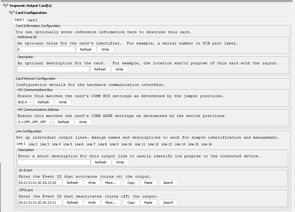
Below are the card dialog configuration options for this card (refer to diagram on right):
After changing fields, click the Write button to save the changes.
| CDI Group | CDI Field | Choices | Comments |
|---|---|---|---|
| Card Configuration | Reference ID | 0-255 | An optional value for the card’s identifier. For example, a serial number or PCB component label. |
| Card Configuration | Description | Text | You can optionally enter reference information here to describe this card. For example, the location and/or purpose of this card with the layout. |
| Card Network Configuration | HW Communications Bus1 | BUS A, BUS B | Ensure this matches the card’s COMM BUS settings as determined by the jumper positions. |
| Card Network Configuration | HW Communications Address1 | 0 - 7 | Ensure this matches the card’s COMM ADDR settings as determined by the switch positions. |
| Output Lines Configuration | Description | Text | Enter a short description for this output line to easily identify its purpose or the connected device. For example, the location and/or purpose of the line within the layout. |
| Line Configuration | Initial Output State at Power-On | OFF, ON, PERVIOUS | Select the default state of the output line when the system powers on. Options include ‘On’ for an active state, ‘Off’ for an inactive state, and ‘Previous’ to retain the output line’s state from the last session before shutdown. The default setting is ‘Previous’. |
| Line Configuration | On Event ID | Event ID | Enter the Event ID that activates (turns on) the output (HIGH = 5V or 12 VDC). Voltage is based on the card’s VOLTAGE selection. |
| Line Configuration | Off Event ID | Event ID | Enter the Event ID that deactivates (turns off) the output (LOW = no voltage) |
- For details on bus and address selections, refer to HW Communications Configuration
Functional Testing
After configuring your Output Card and ensuring all hardware connections are properly established, it’s essential to verify the functionality of each output line to ensure your setup works as intended for your model railroad automation. Follow these steps to conduct functional testing:
- Generate Event IDs: To test each output line, activate them by producing the corresponding Event IDs. Event IDs can be generated and sent through various methods, including:
- JMRI Send Frame tool, refer to Sending Events.
- Configured input/sensor cards (e.g. Button Card).
This flexibility allows you to simulate real-world operation scenarios and control actions in your train layout.
- Verify Device Behavior: Once the Event IDs are sent, observe the behavior of each connected device. Ensure that every device responds as expected, based on the configured LCC events. This step is crucial for validating that the Output Card and the devices it controls are properly integrated into your LCC system and that they operate correctly within the context of your model railroad.
Troubleshooting Guide
| Issue | Possible Cause | Solution |
|---|---|---|
| Output not responding | Incorrect Event ID configuration | Verify the Event IDs are correctly set in the configuration tool. |
| LED not lighting up | LED is burned out, voltage mismatch, or LED polarity | Test the LED with a battery to ensure it’s functional. If it’s not working, incorporate a current-limiting resistor in the circuit. Optionally, utilize the Output Card’s resistors by deactivating the BYPASS RESISTOR switch (SW2, SW3). Check that the VOLTAGE (JP5) jumper setting on the Output Card corresponds with the device’s voltage requirements. Verify the LED’s orientation by ensuring its cathode is connected to the ground, either through the breakout card’s GND connector or by linking to LINE 16 on the Output Card (JP3 set to GND). |
| Device overheats | Exceeding current limit | Check if the device’s current requirement exceeds the Output Card’s limit. Use current limiting resistors increase the value of the resistors on the card change the VOLTAGE (JP5) to 5V. |
| Card is not connecting | Incorrect HW Communications Bus and Address | Confirm the HW Communications Bus and Address matches between the card and the configuration tool. If encountering this, check that the HW Communications Bus and Address settings align between the card and the configuration tool. Utilize the LCC Fusion Node Cluster Serial Monitor to inspect currently detected I2C devices within the LCC Fusion Node Cluster network. |