Soldering Tips
Table of contents
Table of contents
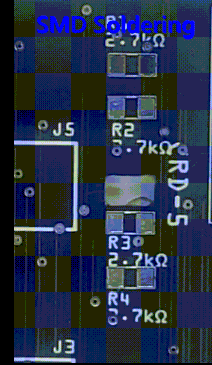
SMD Soldering
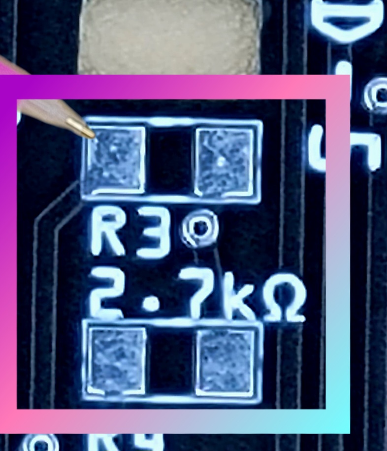 SMD Soldering involves soldering SMD component’s pads to the corresponding pad on the PCB. As with all component placement, refer to the component designator found near the pad for information. In the picture on the right, the R3 has 2 pads for a 2.7kΩ resistor (1206 SMD). Some PCBs have a large number of similar components leading to difficulty in matching component pads to designators. this is especially true for the resistors, capacitors, and LEDs that use the same package (SMD 1206) and therefore the pads are the same.
Recommendations:``
-
Personal Safety and Protection
-
When soldering use eye protection such as safety glasses. These should comfortable and clear. Magnification is useful for placement of the small SMD components. See PCB Tools.
-
Soldering produces harmful fumes that should be vented away using a fan or preferably a soldering fumes extractor (fan with a filter). See PCB Tools
-
Protect your work surface using a heat resistant mat or pad. Recommend using a silicone solder mat. See PCB Tools.
-
-
Solder Paste Applicator:
 When soldering a PCB such as the Node Bus Hub with a small number of SMD components and no SMD IC, consider using a solder paste applicator. Use of the syringe version with a small tip provides easy placement of the solder directly on the pad. Optionally use a extruder to control the flow from the syringe. See PCB Tools
-
Stencil Usage:
-
A solder stencil is a metal sheet provided by fabricators ($$) when ordering a PCB. The metal sheet provides cutouts at the exact location of all of the solder pads for the SMD components.
-
Utilize the stencil for applying solder paste to SMD pads. This guarantees the appropriate amount of solder is used, minimizing the risk of solder bridges and excess solder balls.
Recommend using a stencil when reflow soldering a PCB containing a large number of SMD components or SMD IC component (very small solder pads).
-
When ordering your PCB from the fabricator (like JLCPCB), also order the stencil for the board. This ensures precise application of solder paste.
-
Align the stencil onto the PCB using the two small ‘tooling holes’ located in its upper and lower corners. These holes are designed to fit a push pin.
-
To keep the stencil steady on the PCB while applying paste:
-
When the PCB has Tooling Holes, insert a push pin through the hole in the stencil and PCB into a soft base align the stencil on the PCB and hold it in place while applying solder.
Tooling Holes are available with some PCB, usually found as two holes at the outer edges, both thru the stencil and the PCB.
-
Place the PCB on a metal plate, align the stencil using a push pin, and use magnets to secure the stencil on the PCB.
-
For assembling multiple PCBs, it is advisable to use PCB stencils. This approach not only accelerates the assembly process but also enhances the overall quality.
-
- Placing SMD Components:
- It’s recommended to use small containers for holding and labeling each component. Look for small screw-top containers typically used in hobby stores for bead organization.
- Employ fine-tipped, non-magnetic tweezers for picking up and positioning components onto the paste.
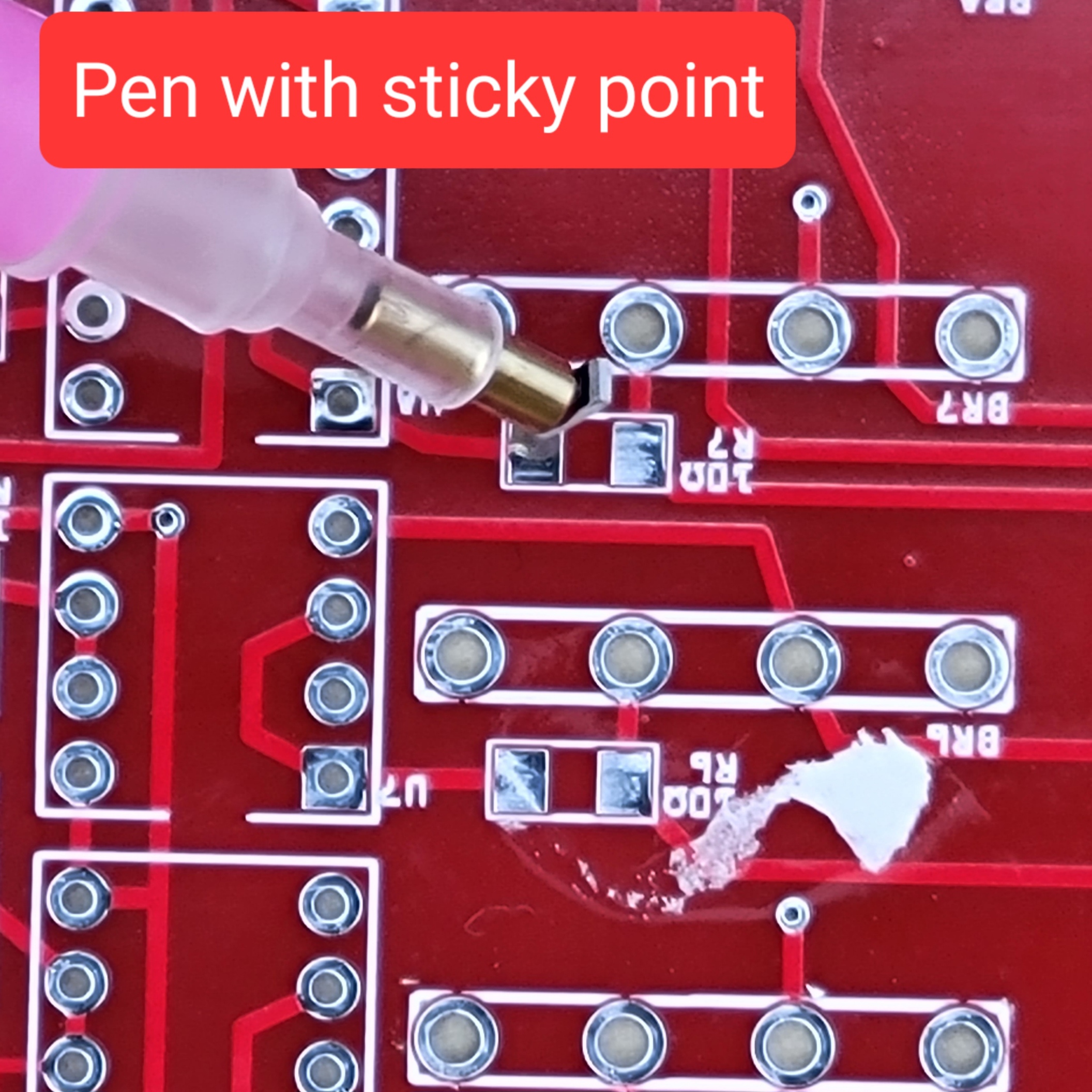 For smaller components, consider using Diamond Art Pens. Their sticky tips provide a comfortable, efficient alternative to tweezers for picking up and placing components.
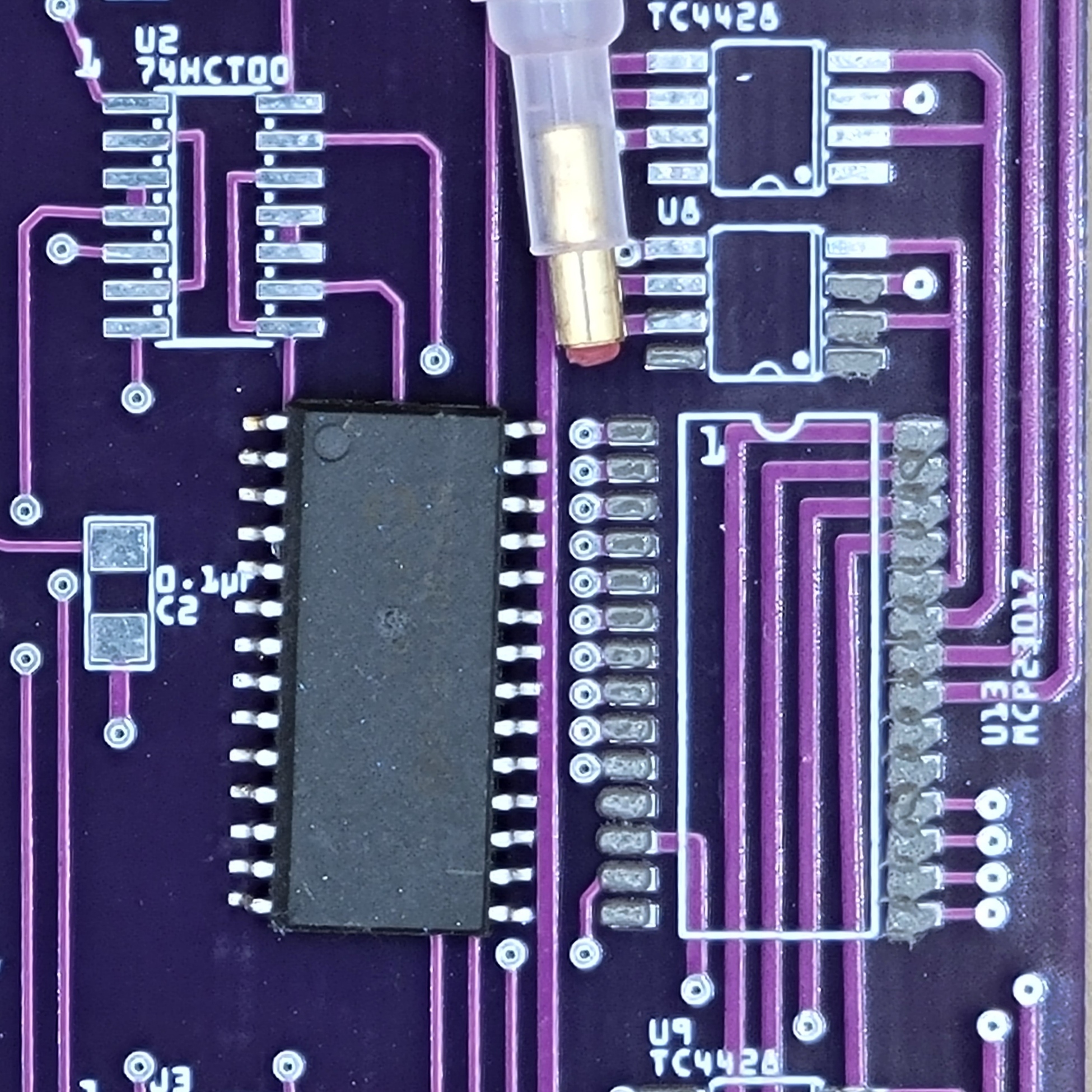 Both the MCP23017 and M54562FP integrated circuits are marked with a small dimple at one corner, signifying pin 1. When positioning these ICs on their respective PCB symbols, ensure that pin 1 aligns with the end of the symbol that also features a dimple representation. Refer to the provided example on the right, where the IC displays a dimple in its upper left corner. This corner should be aligned with the corresponding dimple-end on the silkscreen.
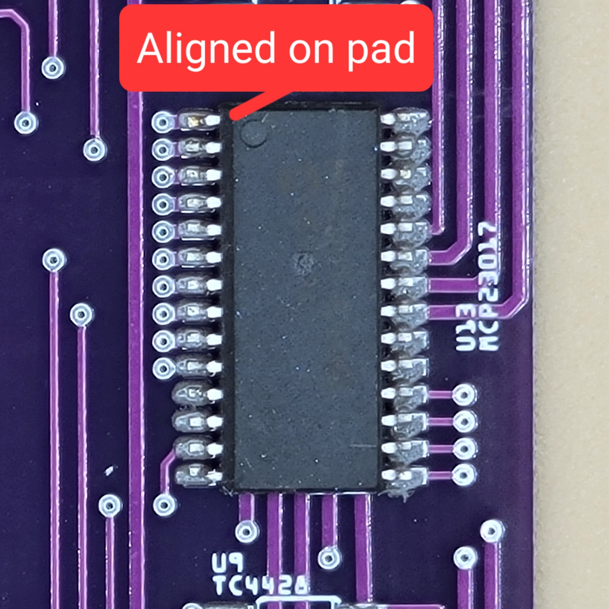 After placing an IC in the solder paste, insure that the IC pins are aligned exactly on top of the pad. If the IC pins are very closely centered, later during the reflowing the IC will float into it’s final position, centered on top of the pads.
When handling small SMD components, it is recommended to use a hobby pen with a sticky tip for ease of placement.
- PCB Prep:
- Use alcohol before and after soldering to remove residues
- Reflow Soldering Process
- Once the solder paste is applied to the PCB and components are placed, proceed with one of the following methods:
- Best Employ a countertop oven or hot plate for the reflow process. The specific time and temperature settings will depend on the solder paste’s melting point. For instance, with a solder paste that melts at 278°F, a typical reflow cycle in a countertop oven would be 4 minutes at 400°F, including preheating.
- Low Cost Utilize the Hot Air Pencil (or Soldering Iron) from a reflow station. Set the air flow to a low level and position the pencil just above the SMD component, gently swirling the air around it. This process helps the SMD align and settle onto the pads as the paste melts, transforming from a dark gray to a shiny silver finish.
- Lowest Cost Use the soldering iron tip to heat the solder paste while holding the component in place. This method takes more time, but works well. For IC’s, consider loading the tip with solder and then swiping along the IC’s pins. Clean the tip and then swipe the soldering iron tip out and away from the IC to remove solder bridges.
To reclaim SMD components from a PCB or adjust their position, reheating the board is effective. This can be achieved using a hot plate, countertop oven, or a Hot Air Pencil.
- Soldering Through-Hole Technology (PTH)
- For optimal results, employ a solder with a low melting point, approximately 360°F, and use a soldering iron with an oblique tip.
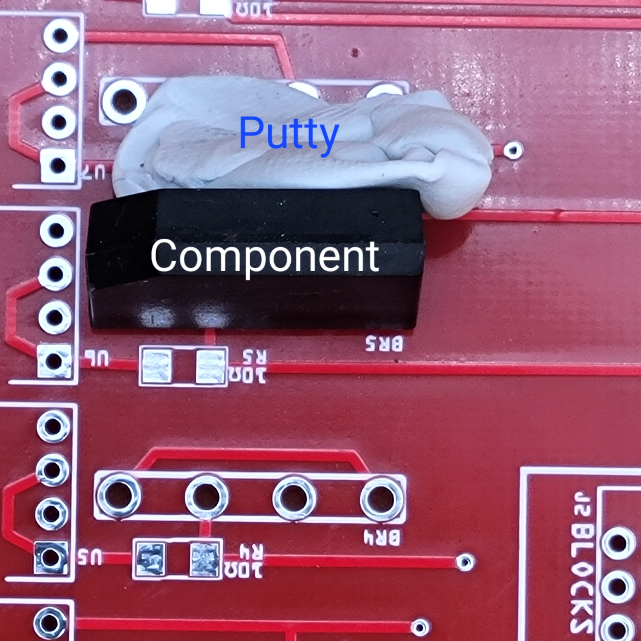 Securely position and maintain the component in its place. Tip: Tacky putty can be effective in holding the component steady on the top side of the PCB while you solder from the underside.
- Initiate soldering at the pin’s base, moving the iron upwards to draw the solder along the pin’s length.
- To ensure the component is fully seated on the PCB, begin by soldering just one pin of the PTH component. While reheating this pin, adjust the component to its final position. Once in place, proceed to solder the remaining pins.
- Use a solder tip cleaner (brass sponge is best) to frequently to clean the soldering tip. Regular cleaning, before and after soldering sessions, prevents oxidation build-up and extends the tip’s life, making soldering more effective and producing cleaner, more reliable connections.
For reclaiming PTH components, utilize a solder removal tool, such as a ribbon or de-soldering vacuum pump, in conjunction with reheating the solder.