PWM Card Assembly Guide
Table of contents
Table of contents
Introduction
See the How to Use Assembly Guides for detailed instructions.
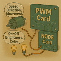
The PWM (Pulse Width Modulation) Card, in synergy with the LCC Fusion Node Card, forms the signaling and motor control backbone of the LCC Fusion Project system, controlling signal lamps and motors.
For example, when controlling signals, upon detecting a train within a block, a BOD Card generates an LCC event, signaling the occupancy status. This event is captured by the LCC Node, which, depending on the setup, could trigger various responses such as activating the PWM Card. This activation allows for nuanced control over railroad signals and other trackside functionalities, enhancing the realism and operational efficiency of the model railroad environment.
The PWM Card hardware configuration includes:
- network cable sockets for up to 16 output lines
- selection of the communication bus (BUS or BUS B)
- selection of the communication address (0-7)
- selection of 5V or 12 VDC for lines 7/8 and 15/16 when they are configured for PWR
- selection of whether Lines 7/8 & Lines 15/16 are to be used for output or PWR (5 VDC/12 VDC)
flowchart LR
can["CAN Network"];
subgraph layout ["Train Layout"];
  direction LR;
  can --> |"LCC Event<br/>(on/off)"| n["Node Card"];
  n -->|"PWM Signal, <br/> Digital Output (high/low)"| c["PWM Card (16x)"];

  c --> |"PWM Signal <br/> LED Control (on/off/brightness)"| bb1["Digital I/O<br/>Breakout Board"];
  bb1 -.- led(("LED <br/> (8x)"));

  c --> |"PWM Signal, <br/> (speed/direction)"| bb2["DC Motor Driver<br/>Breakout Board"];
  bb2 -.-|"Motor Control (speed/direction)"| dcmotor(("DC Motor <br/> (2x)"));

  c --> bb3["Servo Motor Driver<br>Breakout Board"];
  bb3 -.- |"Servo Control, <br/> (position)"| servo(("Servo Motor Driver<br/>Breakout Board (8x)"));
end
classDef lSalmonStyle fill:#FFA07A,stroke:#333,stroke-width:2px,font-size:24px;
class c lSalmonStyle;
classDef lightGrayStyle fill:#d3d3d3,stroke:#333,stroke-width:2px,font-size:24px;
class layout lightGrayStyle;
Safety Precautions
- See Safety Precautions.
Assembly-Configuration Options
The PWM Card supports only one assembly configuration with all of the following components installed.
The ESD protection diode D18 is recommended, but not required.
Assembly and Component Placement
This section combines both the component specifications and the assembly instructions to ensure a smooth assembly process. Below is a comprehensive list of components, their placement on the PCB, and orientation details to assist you during assembly.
High-Level Steps for Assembly:
- PCB for the card can be ordered from any PCB fabricator using these Gerber Files.
- Clean PCB with alcohol to remove residue. See Cleaning_PCB for details.
- See also: Soldering Tips
- PCB Components - listing of components used for PCB assembly
- PCB Parts - listing of parts used for PCB assembly
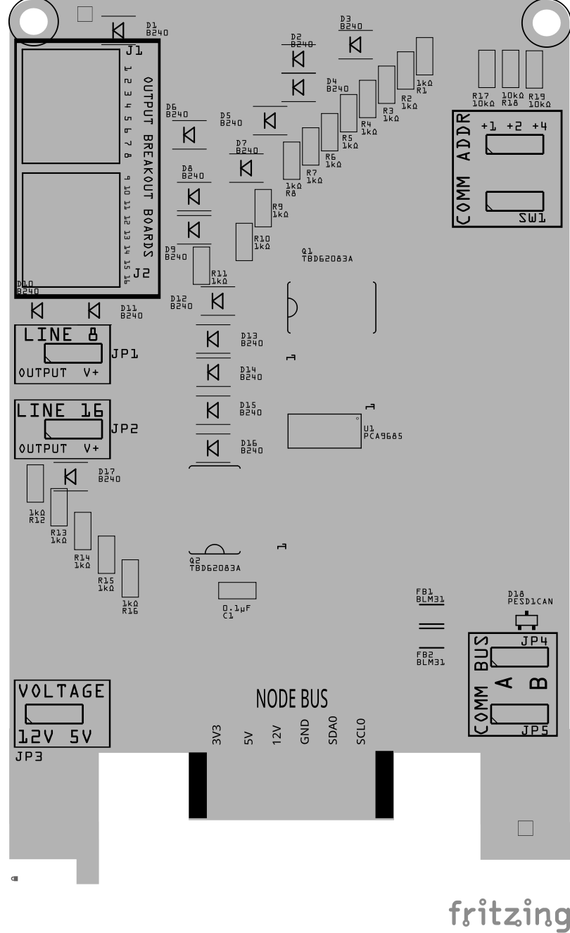
Below is a list of the PCB components used for this card (see diagram before reference):
![]()
![]()
| Component Identifier | Count | Type | Value | Package | Purpose | Orientation |
|---|---|---|---|---|---|---|
| C1 | 1 | Capacitor-Ceramic | 0.01 uF | 1206 X7R | Used to condition/filter the current for the IC | None |
| D1 - D17 | 17 | Diode-Schottky | SS310 | SMD | Protection against reverse current to ground connections | Cathode end has a white line and positioned towards PCB left edge |
| D18 | 1 | ESD Diode | PESD1CAN | SOT-23 SMD | I2C data bus electrostatic discharge (ESD) protection | Fits only one way |
| FB1, FB2 | 2 | Ferrite Bead | BLM31PG121SN1L | 1206 SMD | I2C Data Line Noise Suppression Ferrite Bead | None |
| J1, J2 | 2 | Connector | RJ45 socket (8P8C) | PTH | Network cable (CAT5/6) connection to (1 or 2) breakout boards (e.g. Signal Masts Breakout Board) | Fits only one way |
| Selectors | ||||||
| JP1, JP2 | 4 | Male Header | 3-Pin | 2.54mm PTH | Use for setting Lines 7/8 & Lines 15/16 to operate as either PWM Output, or as PWR (GND with 5 VDC or 12 VDC based on the PWR OUT selection) | None |
| JP3 | 1 | Male Header | 3-Pin | 2.54mm PTH | Used for setting of the output voltage for lines 7/8 and 15/16, when the lines are configured for PWR mode | None |
| JP4, JP5 | 2 | Male Header | 3-Pin | 2.54mm PTH | Used for COMM BUS selection (I2C hardware bus) for either BUS A or BUS B. These are the ESP32 hardware buses used for serial comms | None |
| SH1 - SH5 | 5 | Jumper Cap | 2.54mm | N/A | Used with I2C Bus and Vcc selections. Recommend tall caps for ease of use | None |
| R1-R16 | 16 | Resistor | 1KΩ | 1206 SMD | Used to limit the current thru the output lines | None |
| R17 - R19 | 3 | Resistor | 10KΩ | 1206 SMD | Used to limit the current for the BUS ADDR lines | None |
| SW1 | 1 | DIP Switch | 3-Pin | 2.54mm PTH | Used for COMM ADDR selection (I2C address offset, 0-7). This offset is added to the I2C base address of the MCP23017 IC (0x20) | Position so switch so ON is towards PCB top edge |
| U1 | 1 | IC | PCA9685 | TSSOP28 SMD | PWM Expander using I2C serial interface to control 16 PWM pins, each connected to an output line | IC indent (pin 1) is positioned towards PCB left edge |
| Q1, Q2 | 2 | IC | TBD62083 | SOIC-18/SOP-18 | Darlington Transistor Array for switching supply voltage to the output lines. Controlled by the PCA9685 IC signals | IC indent (pin 1) is positioned towards PCB bottom edge |
Tools Required
For a list of recommended tools, refer to List of recommended tools.
Testing and Verification
Visual Inspection
-
Initial Check: Examine the board for any obvious issues like missing components, solder bridges, or components that are misaligned or not fully seated.
-
Solder Join Inspection: Use a magnifying glass or a microscope to inspect solder joints. Look for cold solder joints, insufficient or excessive solder, or any shorts between pads.
-
Component Orientation: the IC’s are correctly oriented according to the PCB silkscreen or schematic.
Connectivity Testing
Continuity Check: Use a multimeter in continuity mode to check for shorts between power rails and ground, and to ensure there are no open circuits in critical connections.
Card Configuration Settings
-
The following test and verifications of the card should be performed after a through inspection of the card’s soldering. Check all of the PTH component pins and SMD pads. Make sure there are no solder bridges between pins and pads.
-
Configure the PWM Card:
-
Select the
COMM BUSby positioning (2) Jumper Caps on eitherAorBmale header pins (JP1, JP2) -
Select the
COMM ADDRESSswitch (SW1) by sliding each of the 3 switches to either theONorOFFposition. Setting a switch to ON increments the address by 1, 2, or 4 for an address range of 0 to 7. Up to 8 devices can then be configured forAand 8 forB. -
Select the
LINES 15/16function to bePWMto verify the connection to an LED works.Later change
LINE 15/16selector toPWRto test using line 16 for completing the circuit for the LEDs
-
Power-Up Tests
- Assembly a tested Power Module to the LCC Fusion Node Card.
- Apply Power to the Power Module and verify the following:
- Check for Hot Components: Feel for components that are overheating, which could indicate a problem like a short circuit or incorrect component.
Functional Testing
Functional testing of the card can be performed after completing the power-up testing. Testing consists of testing network communiations, followed by controling signal lamps (LEDs).
HW Communications Testing
Communications testing verifies the LCC Node can communicate with the BOD Card’s I2C IC via the Node Bus Hub connections. This is performed using the LCC Fusion Node Card’s testing firmware and a serial monitor.
-
Insert the PWM Card into a Node Bus Hub along with a LCC Fusion Node Card.
-
Install LCC Fusion Project firmware that includes serial monitor for testing.
-
Verify that the I2C connection between the LCC Fusion Node Card and the PWM Card work.
See Testing I2C Cards for details on how to test the communications for a I2C enabled card.
PWM IC Testing
After hardware communication has been established, verify the PWM IC is able to drive LED devices using a Signal Masts Breakout Board. Use the Node’s serial monitor to simulate an output request to drive of the PWM Card’s output pins to an LED connected to the Signal Masts Breakout Board as follows:
- In the serial monitor’s input, enter
Mfor the LCC Node’s serial monitor Main Menu. - Select
[1] Node Managementand[1] Device Testing Management - Select
[5] Simlulate PWM Device Output - From the list of MCP devices, select the device # for the PWM Card being tested
- Enter the number for the pin to tested.
- Verify the output device (LED) is turned on
- Repeat for each of the output lines
Provisioning the Card
- See Provisioning a Card.
Troubleshooting
- See I2C Trouble Shooting.
Appendences
PCB Specifications
Specifications for the card include:
![]()
| Characteristic | Value |
|---|---|
| Max output lines | 16 |
| Maximum Number of Cards per LCC Fusion Node Cluster | 161 |
| Max Current per line (TBD62063 transistor limit) | 500 mA |
| Max Current all lines (Node Bus Hub limit) | 1.5A |
- The LCC Fusion Node Cluster can support up to 16 cards, distributed across two I2C hardware buses, with a maximum of 8 cards per bus.
- Note: total includes all cards using the I2C address range of
0x40(PCA9685 IC).
- Note: total includes all cards using the I2C address range of
How It Works
This section delves into how the PWM Card operates within the system:
At its core, the PWM Card’s operation is orchestrated through the LCC Fusion Node Card’s firmware, which communicates with the PCA9685 IC— a crucial port expander on the PWM Card. This interaction is facilitated through specific bus and address settings detailed in the CDI I2C section of the card.
Upon receiving instructions to activate (set HIGH) or deactivate (set LOW) a pin, the PCA9685 IC controls a corresponding darlington transistor (TBD62034). This transistor, in turn, manages the switching of an output line on or off.
To tailor the PWM Card’s behavior to specific needs, Jumper Caps are employed to configure the selection pins as outlined below:
| Selector Label | Components Indicator | Options | Description |
|---|---|---|---|
LINES 7/8 |
JP1 | PWM, PWR |
Configures lines 7/8 for either: - PWM mode, where it behaves like the other PWM output lines.- PWR mode, serving as a GND and voltage connection to the breakout board for use with lines 1-7. Use PWR mode when external devices or LEDs on these lines need a power source. |
LINES 15/16 |
JP2 | PWM, PWR |
Configures lines 15/16 for either: - PWM mode, where it behaves like the other PWM output lines.- PWR mode, serving as a GND and voltage connection to the breakout board for use with lines 1-14. Use PWR mode when external devices or LEDs on these lines need a power source. |
PWR OUT |
JP3 | 12 VDC, 5 VDC |
Selects the voltage level for the PWR option (when PWR is selected on Line 7/8 or Lines 15/16). This setting applies only to lines configured in PWR mode and does not affect lines in PWM mode. |
The card utilizes current-limiting resistors for each line to manage device output current. The default resistor value is marked for creating about 50% LED brightness, but this can be adjusted by replacing the resistor for each line to suit specific requirements.
PCB Protection
To ensure the reliable operation and longevity of your PWM Card, several protection components have been integrated. These components safeguard the PWM Card from overcurrent, voltage spikes, and electrical noise. Below is a brief overview of each protection element and its role:
![]()
| Protected Component | Protection Component | Function | Specifications | Location |
|---|---|---|---|---|
| TBD62083 IC | Decoupling Capacitor 0.1 µF | Filters out high-frequency noise and transient voltage spikes from the power supply, ensuring a stable voltage for the MCP23017. | Value: 0.1 µF | Across Vcc and GND near the MCP23017 |
| I2C Lines from LCC Fusion Node Bus Hub | Ferrite Bead BLM31PG121SN1L | Provides high-frequency noise suppression on the I2C lines. | Impedance: 120 ohms at 100 MHz | In series with the SDA and SCL lines of the I2C bus |
| I2C Lines from LCC Fusion Node Bus Hub | ESD Protection Diode PESD1CAN | Protects the I2C lines from electrostatic discharge and voltage spikes. | Reverse Stand-off Voltage (Vr): 24 VDC Clamping Voltage (Vc): 40 VDC |
Across the SDA and SCL lines from the card’s edge connector to GND, near the MCP23017. |
| Output Lines | SS310 Diodes | Protect against reverse voltage by blocking current flow in the wrong direction. | Reverse Voltage: 100 VDC Forward Current: 3A |
Clamping diode In series with all output lines |
References
- I2C Output Mapping (PWM Card)
The PWM Card uses a PCA9685 to generate 8 independent PWM signals. Each line corresponds to one output line on the PCA9685. Output voltage is either 5V or 12V, depending on configuration.
| RJ45 Line | PCA9685 Channel | Direction | Voltage Level | Logic Levels | Purpose | Notes |
|---|---|---|---|---|---|---|
| L1 | CH0 | Output | 5V/12V PWM | HIGH = ON (PWM > 0) | PWM Output 1 | Drives LED, motor, or other load |
| L2 | CH1 | Output | 5V/12V PWM | HIGH = ON (PWM > 0) | PWM Output 2 | |
| L3 | CH2 | Output | 5V/12V PWM | HIGH = ON (PWM > 0) | PWM Output 3 | |
| L4 | CH3 | Output | 5V/12V PWM | HIGH = ON (PWM > 0) | PWM Output 4 | |
| L5 | CH4 | Output | 5V/12V PWM | HIGH = ON (PWM > 0) | PWM Output 5 | |
| L6 | CH5 | Output | 5V/12V PWM | HIGH = ON (PWM > 0) | PWM Output 6 | |
| L7 | CH6 | Output | 5V/12V PWM | HIGH = ON (PWM > 0) | PWM Output 7 | |
| L8 | CH7 | Output | 5V/12V PWM | HIGH = ON (PWM > 0) | PWM Output 8 | May share GND depending on config |