Quad-Node Card Assembly Guide
Table of contents
Table of contents
Introduction
See the How to Use Assembly Guides for detailed instructions.
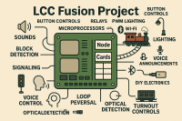
In conjunction with the LCC Fusion Project Node Bus Hub, the Quad-Node Card provides four (4) LCC compatible Nodes. Typically, in an LCC Fusion Project project, the Quad-Node Card is placed into a LCC Fusion Node Cluster using a Node Bus Hub to connect a LCC Fusion Node Card, Power Module, and optional LCC Fusion Project I/O cards.
The LCC Fusion Power-CAN Card can be implemented with a number of optional features:
-
Power Supply options (see Power Module for more details):
-
VIN: CAN serial connection via network cable (CAT5/6) or connectors (JST-XH or spring terminal).
VIN: 12 – 40 VDC DC via network cable (CAT5/6), USB-C-form socket, 5557 ATX connector, or DC-005 barrel jack.
- Accepts fixed-voltage laptop-style power supplies:
- 18 – 20 VDC DC at up to 3 A
- Either barrel plug (2.1 mm center-positive) or USB-C-form connector
- PD-compliant power supplies may also be used with a PD trigger/decoy module connected to the ATX-IN connector.
- This is a DC power input only – not a USB-C data or PD port.
- Do NOT connect directly to computers, phones, or PD chargers.
- Accepts fixed-voltage laptop-style power supplies:
-
-
Output Power:
- VOUT: 12 VDC - 40 VDC DC via USB-C or 5557 ATX connection for powering other LCC Fusion Node Cards or Power-CAN Cards.
- VOUT: 5 VDC DC via USB-C for powering low voltage devices (e.g. RPI).
-
CANable adapter for Windows USB to CAN connection for JMRI integration.
-
LCC Fusion Node Bus Hub(RJ45) network cable connection to connect with a remote LCC Fusion Project Node Bus Hub
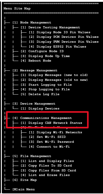
CAN Communications
The LCC Fusion Power-CAN Card connects to a CAN Network, enabling communication of LCC Events. It features two RJ45 sockets for easy in/out connections, allowing multiple Node Cards to be daisy-chained together.
Below is a diagram illustrating the daisy-chaining of Power-CAN Card with a Node Card via their RJ45 sockets:
flowchart LR;
subgraph hub["Node Bus Hub"];
direction LR;
 pccard["Power-CAN Card"];
end;

can["CAN Network"];
can <-.-> |"Network Cable"| pccard;
pccard <-.-> |"Network Cable"| nodecard["Node Card"]

classDef lSalmonStyle fill:#FFA07A,stroke:#333,stroke-width:2px,font-size:24px;
class pccard lSalmonStyle;
classDef lightGrayStyle fill:#d3d3d3,stroke:#333,stroke-width:2px,font-size:24px;
class can lightGrayStyle;
Assembly-Configuration Options
The Quad Node Card supports multiple assembly configurations to fit various use cases.
![]()
| Configuration | Required/Optional | Description | Required Components | Optional Components | |||
|---|---|---|---|---|---|---|---|
| ESP32 Module Support | Required (at least one | Provides support for attaching an Super-Mini ESP32-S3 Module | See table below for components required for each ESP32 installed | None | |||
| CAN Termination Support | Required | I2C Low Voltage Dection and Correction | • Voltage Comparator (U5, ZD1, R33, R34) • 120Ω Switching Circuit R35, R36, C10, Q1, Q2) |
None | |||
| CAN Bus Protection | Required | Provides ESD and noise filter support for CAN Bus | • Noise Suppression: ferrite beads FB1 and FB2 | • ESD Protection: diode D3 | |||
| I2C Bus Protection | Required | Provides ESD and noise filter support for I2C Bus | • Noise Suppression: ferrite beads FB3-FB6 | • ESD Protection: diode D50,D51 | |||
| Alert Buzzer | Optional | Provides buzzer support for firmware generated alerts | • Buzzer: buzzer SG1 Protection:** diodes D52 - D55 |
None | |||
| Optional ESP32 Module Support | MCU, Socket Headers | CAN IC | Resistors (optional) | Capacitors | Clamping Diodes | ESD Diode | Connector / Selector |
| 1 | U6, J5 (2x 8-pin female header) | U1 | R1-R8 | C1, C2 | D1-D8 | D33-D36 | J1, JP1 |
| 2 | U7, J6 (2x 8-pin female header) | U2 | C3, C4 | D9-D16 | D37-D40 | J2, JP2 | |
| 3 | U8, J7 (2x 8-pin female header) | U3 | R17-R24 | C5, C6 | D17-D24 | D41-D44 | J3, JP3 |
| 4 | U9, J8 (2x 8-pin female header) | U4 | R25-R32 | C7, C8 | D25-D32 | D45-D48 | J4, JP4 |
Assembly and Component Placement
This section combines both the component specifications and the assembly instructions to ensure a smooth assembly process. Below is a comprehensive list of components, their placement on the PCB, and orientation details to assist you during assembly.
High-Level Steps for Assembly:
- PCB for the card can be ordered from any PCB fabricator using these Gerber Files.
- Clean PCB with alcohol to remove residue. See Cleaning_PCB for details.
- See also: Soldering Tips
- PCB Components - listing of components used for PCB assembly
- PCB Parts - listing of parts used for PCB assembly
Below is a list of the PCB components used for this card (see diagram before reference):
![]()

![]()
| Component Identifier | Count | Type | Value/Description | Package | Purpose | Orientation |
|---|---|---|---|---|---|---|
| Capacitors | ||||||
| C1, C3, C5, C7, C9 | 5 | Capacitor-Ceramic | 0.1uF | 1206 X7R | IC protection | None |
| C2, C4, C6, C8 | 4 | Capacitor-Ceramic | 10uF | 1206 X7R | IC protection | None |
| C9 | 1 | Capacitor-Ceramic | 0.1uF | 1206 X7R | Filters high-frequency noise from CAN signals, smoothing the voltage for the comparator | None |
| C10 | 1 | Capacitor-Ceramic | 47nF | 1206 X7R | Filters high-frequency noise from CAN-H and CAN-L lines | None |
| Diodes | ||||||
| D1 - D32 | 32 | TVS Diode | SMAJ5A | SMA | GPIO pin Transient Voltage Spike (TVS) protection | Cathode end has a white line and positioned towards PCB left edge |
| D33 - D48 | 16 | ESD Diode | PESD1CAN | SOT-23 SMD | GPIO pin electrostatic discharge (ESD) protection | Fits only one way |
| D49 | 1 | ESD Diode | PESD1CAN | SOT-23 SMD | CAN Network Bus electrostatic discharge (ESD) protection | Fits only one way |
| D50, D51 | 2 | ESD Diode | PESD1CAN | SOT-23 SMD | I2C data bus electrostatic discharge (ESD) protection | Cathode end has a white line and positioned towards PCB bottom edge |
| D52 - D55 | 4 | Diode-Schottky | SS310 | SMA | Required when installing Buzzer (SG1) | None |
| ZD1 | 1 | Diode-Zener | 2.4 VDC | BZT52 | Required to create a reference voltage | Cathode end has a white line and positioned towards PCB right edge |
| Filters & Noise Suppression | ||||||
| FB1, FB2 | 2 | Ferrite Bead | BLM31PG121SN1L | 1206 SMD | CAN Network Bus Data Line Noise Suppression Ferrite Bead | None |
| FB3 - FB6 | 4 | Ferrite Bead | BLM31PG121SN1L | 1206 SMD | I2C Data Line Noise Suppression Ferrite Bead | None |
| Connectors | ||||||
| J1 - J4 | 4 | RJ45 Socket | 8P8C | PTH | Network cable (CAT5/6) connection to I/O devices | Fits only one way |
| J5 - J8 | 4 | Female Headers | 9-Pin | PTH | Socket for Super-Mini ESP32-S3 development board(s) | None |
| Resistors | ||||||
| R1 - R32 | 32 | Resistor | 1kΩ | 1206 SMD | Current limiting protection for GPIO pin | None |
| R33 | 1 | Resistor | 1kΩ | 1206 SMD | Current limiting for reference voltage | None |
| R34 | 1 | Resistor | 100Ω | 1206 SMD | Low Pass Filter for low signal detection | None |
| R35, R36 | 2 | Resistor | 60Ω | 1206 SMD | CAN network (split) termination circuit | None |
| R37-R40 | 4 | Resistor | 47Ω | 1206 SMD | Edge damping of I2C data lines | None |
| R41-R42 | 2 | Resistor | 47Ω | 1206 SMD | Edge damping of CAN bus lines | None |
| Selectors & Indicators | ||||||
| JP1 - JP4 | 4 | Male Pin Header | 3-Pin | PTH | Line 8 selection (GND or I/O line) | None |
| SH1-SH4 | 4 | Jumper Cap | 2.54mm | — | Use with JP1-JP4 | None |
| LED1 | 1 | LED | Red | 1206 SMD | Alert indicator | Reference back of LED, position cathode towards PCB top edge |
| SG1 | 1 | Buzzer | 3V, Active | MLT-9650, SMD | Used for audio indication of status (error, warning, etc) | None |
| ICs | ||||||
| U1 - U4 | 4 | CAN Transceiver | SN65HVD233DR | SMD | CAN Transceiver for use with ESP32 to provide CAN communications | Package has small dimple in corner (pin 1) which is position to PCB top right edges |
| U5 | 1 | IC (Voltage Comparator) | LM393 or LM2903N | SO-8, SMD | Used for detecting low voltage in the I2C lines (less than 2.4 VDC) | Position IC’s dent towards PCB top/left edges |
| U6, U7, U8, U9 | 4 | MCU (Processor) | ESP32-S3 SuperMini Development Board | PTH, 8-Pin | MCU (processor) for the Quad-Node Card Firmware | Position Super-Mini ESP32-S3 development board’s USB connector to PCB right edge |
| Transistors | ||||||
| Q1, Q2 | 2 | NPN Transistor | BSS138 | SOT-23 | Controls CAN connections to terminator | Fits only one way |
Tools Required
Safety Precautions
- See Safety Precautions.
Testing and Verification
Card Configuration
Visual Inspection
-
Initial Check: Examine the board for any obvious issues like missing components, solder bridges, or components that are misaligned or not fully seated.
-
Solder Joint Inspection: Use a magnifying glass or a microscope to inspect solder joints. Look for cold solder joints, insufficient or excessive solder, or any shorts between pads.
-
Component Orientation: the IC’s are correctly oriented according to the PCB silkscreen or schematic.
Connectivity Testing
- Continuity Check: Use a multimeter in continuity mode to check for shorts between power rails and ground, and to ensure there are no open circuits in critical connections.
Power-Up Tests
- Assembly a tested Power Module to the LCC Fusion Quad-Node Card.
- Apply Power to the Power Module and verify the following:
- Use an voltage meeter to check the tabs at the base edge of the LCC Fusion Quad-Node Card verifying 3V3, 5V, and 12 VDC+. If verification fails, there is a component that is not installed correctly, or a solder bridge.
- Remove the power supply and assembly an DevKit-C Module to the LCC Fusion Quad-Node Card.
- Power up the LCC Fusion Quad-Node Card again and verify the red LED power indicator on the DevKit-C Module is on indicating 5V is being supplied to the ESP32.
- Check for Hot Components: Feel for components that are overheating, which could indicate a problem like a short circuit or incorrect component.
Functional Testing
 Using a USB cable, connect the Super-Mini ESP32-S3 module to a computer.
- Install LCC Fusion Project firmware.
- Using a serial monitor, verify the firmware starts correctly.
- Check the LCC Fusion Quad-Node Card’s CAN Network connectivity using the Node’s serial monitor menu.
- Run JMRI LccPro and connect to the CAN Network.
- While using the JMRI LccPro configuration tool, verify that the Node appears in the network of LCC Nodes.
Troubleshooting
- See I2C Trouble Shooting.
Appendences
PCB Specifications
Specifications for the card include:
![]()
| Characteristic | |
|---|---|
| Super-Mini ESP32-S3 Development Boards | 4 |
| Max Input / Output Lines | 16 |
| Max Output Per Line | 12 mA2 |
| Max Input/Output per ESP32-S3 | 120 mA |
| Minimum Current Draw per SuperMini ESP32-S3 Development Boards (idle CPU, no Wi-Fi, no Bluetooth) | 40 mA1 |
| Maximum Current Draw per SuperMini ESP32-S3 Development Boards (active Wi-Fi and Bluetooth) | 500 mA1 |
| Maximum Current Draw per Card (4 boards, active with both Wi-Fi and Bluetooth) | 2A |
-
Maximum current is based on the Node’s firmware configuration (WiFi and BT) and activity (idle/active).
-
Consider using a resistor inline with output lines to LEDs to reduce the current draw. For example, a 150Ω resistor inline with to a Red LED witha forward voltage of 2V reduces the current to about 8.6 mA.
Component Idle Current (mA) Active Current (mA) CPU 40-50 50 Bluetooth 30 60-100 Wi-Fi 80-90 160-260
How It Works
The Quad-Node Card allows up to 4 Super-Mini ESP32-S3 boards to be installed in sockets. Each ESP32 supports 4 I/O lines via a RJ45 socket and I2C to other LCC Fusion Project I/O cards. Each I/O line can be configured independently via the CDI to be digital input, digital output, ADC, touch or PWM. Each set of I/O lines (RJ45 socket) also provides 5V and GND.
The card is connected to the LCC Fusion Node Bus Hub for 5V and 3V3 power, dual I2C, and CAN Network.
Each Super-Mini board can independently use wireless to:
- bridge to the wired CAN Network via the Node Bus Hub
- connect to I/O cards a Node I/O controller
- Bluetooth to LCC Fusion Configuration Tool
- Bluetooth to serial terminal app for monitoring
Auto Termination Circuit for CAN Bus:
The LCC Fusion Node Cards utilize an automatic CAN bus termination circuit to ensure proper signal integrity while avoiding manual jumper settings by the end user. The termination is dynamically activated when necessary, preventing signal reflections that can occur at open-ended or improperly terminated CAN bus lines.
Why Termination is Important:
- The CAN bus requires 120Ω termination resistors at both ends of the network to prevent signal reflections. These reflections can cause data corruption and reduce communication reliability. Without termination, the CAN signals can bounce back along the cable, interfering with valid data transmissions.
- The auto termination circuit monitors the CAN bus and automatically activates termination at the network endpoints, ensuring proper signal termination without user intervention.
How It Works:
- The auto termination circuit uses two BSS138 MOSFETs to control the connection of two 60Ω resistors and a 47nF capacitor across the CAN lines.
Circuit Breakdown:
- CAN-H and CAN-L Termination:
- The termination consists of two 60Ω resistors connected in series between CAN-H and CAN-L. The junction between these resistors is connected to GND through a 47nF capacitor to filter noise and improve signal integrity.
- BSS138 MOSFET Control:
- The two BSS138 MOSFETs control the connection of the 60Ω resistors. When the MOSFETs are turned on, the resistors and capacitor are connected to the CAN bus, providing the required termination.
- The sources of the MOSFETs are connected to the ends of the two 60Ω resistors, while the drains are connected to CAN-H and CAN-L respectively.
- Activation via Comparator:
- The gates of the MOSFETs are controlled by a comparator (LM393), which monitors the CAN bus voltage levels.
- The comparator is set with a 2.4 VDC reference voltage from a Zener diode to detect when the CAN bus reaches the appropriate voltage levels for termination.
- When the bus voltage meets the termination condition, the MOSFET gates are activated, and the termination circuit is connected.
- Capacitor and Noise Filtering:
- The 47nF capacitor at the junction of the two resistors is connected to GND. This capacitor filters out high-frequency noise, ensuring stable CAN bus communication even in the presence of electrical interference.
Advantages:
- Dynamic Activation: The termination circuit is automatically activated only when needed, preventing unnecessary load on the CAN bus during normal operation.
- Simplified Installation: Users do not need to manually configure jumpers or worry about termination placement. The circuit automatically handles termination at the network endpoints.
- Improved Signal Integrity: The use of MOSFETs ensures that termination resistors and the capacitor are only engaged when required, preventing reflections and maintaining optimal signal quality.
Connections
| Component Designator | Connector Label | Connector Type | Connection Number | Function | Description |
|---|---|---|---|---|---|
| NODE BUS | NODE BUS | Card Edge | 1-12 | Power, Communications | Connection to Node Bus Hub |
| J5, J6, J7, J8 | SuperMini ESP32-S3 | 2x 8-Pin Header | 1-8 | ESP32 Module Socket | Connection to SuperMini ESP32-S3 Module |
| J1, J2, J3, J4 | I/O | RJ45 Socket | 1-4 (I/O) 7=5V 8=GND |
I/O Devices | Connection to I/O devices (analog, digital, PWM, touch) |
PCB Protection
The Quad-Node Card integrates multiple Super-Mini ESP32-C3 boards and includes robust protection components to ensure reliable operation. Below is an overview of each protection element integrated into the Quad-Node Card and its role:
![]()
| Protected Component | Protection Component | Function | Specifications | Location |
|---|---|---|---|---|
| Each Super-Mini ESP32-C3 Development Board | Decoupling Capacitors | Filters out high-frequency noise and transient voltage spikes from the power supply, ensuring stable voltage for each ESP32-C3. | Values: 0.1 µF ceramic, 10 µF electrolytic or ceramic | Across Vcc and GND near each ESP32-C3 |
| ESP32 GPIO | TVS Diode & Series Resistor Network (with SS310 diode) | Clamps transient overvoltages, filters high-frequency noise, and blocks reverse current from the buzzer to protect the GPIO pin. | Reverse Voltage: 100 V (max) Forward Current: 3 A (transient rating) |
Inline between the ESP32 GPIO and the buzzer’s 3V connector (series resistor and diode network) |
| CAN Bus (each set) | Automatic Termination | Provides proper termination to prevent signal reflections on the CAN bus. | Value: 2x 60 Ω in series (120 Ω) | Across CANH and CANL lines, automatically applied based on CAN network voltage while using a low-pass filter to measure peak voltage. |
| CAN Bus (each set) | ESD Protection Diode PESD1CAN | Protects the CAN bus lines from electrostatic discharge and voltage spikes. | Reverse Stand-off Voltage (Vr): 24 VDC Clamping Voltage (Vc): 40 VDC |
Across CANH to GND and CANL to GND |
| CAN Bus | Series Damping Resistor | Slows edge-rates and dampens reflections on long I²C runs (>100 mm), improving signal integrity. | Value: 47 Ω (1206) | In series CANH/CANL lines at transceiver pins |
| I2C Trunk Feed | Series Damping Resistor | Slows edge-rates and dampens reflections on long I²C runs (>100 mm), improving signal integrity. | Value: 47 Ω (1206) | In series with SDA and SCL at the ESP32 I2C out |
| I2C Lines | Ferrite Bead BLM31PG121SN1L | Provides high-frequency noise suppression on the I2C lines. | Impedance: 120 Ω at 100 MHz | In series with the SDA and SCL lines of the I2C bus |
| I2C Lines | ESD Protection Diode PESD1CAN | Protects the I2C lines from electrostatic discharge and voltage spikes. | Reverse Stand-off Voltage (Vr): 24 VDC Clamping Voltage (Vc): 40 VDC |
Across the SDA and SCL lines to GND |
| GPIO to RJ45 Sockets | Current Limiting Resistor | Limits current to protect GPIO pins from accidental shorts. | Value: 1kΩ | In series with each GPIO pin |
| GPIO to RJ45 Sockets | ESD Protection Diode PESD1CAN | Protects two GPIO pins from electrostatic discharge and voltage spikes. | Reverse Stand-off Voltage (Vr): 24 VDC Clamping Voltage (Vc): 40 VDC |
Pin 1 to GPIO1, Pin 2 to GND, Pin 3 to GPIO2 |
| GPIO to RJ45 Sockets | TVS Diode SMAJ5A | Clamps high-voltage transients to protect GPIO pins. | Stand-off Voltage: 5V Clamping Voltage: 9.2 VDC |
Across each GPIO pin to GND |
| GPIO to RJ45 Sockets | RJ45 Sockets | Connect 8 GPIO pins from each Super-Mini ESP32-C3 for I/O purposes. | Pins: 8 | Connected to each set of Super-Mini ESP32-C3 pins |
| Ground Bus | 48mil Ground Bus | Provides a low-resistance path for all protection components, ensuring effective grounding and noise suppression. | Width: 48 mil | Used by all protection components |
Summary These protection components work together to safeguard the Quad-Node Card from various electrical faults. The decoupling capacitors filter out noise and transient voltage spikes, ensuring stable power for each Super-Mini ESP32-C3. The jumper-selectable termination resistor, made of two 60Ω resistors in series, ensures proper signal integrity on the CAN bus by allowing termination to be enabled or disabled as needed, while the ESD protection diodes protect the CAN and I2C lines from voltage spikes and electrostatic discharge. The ferrite bead suppresses high-frequency noise on the I2C lines. The current limiting resistors, ESD protection diodes, and TVS diodes protect the GPIO pins connected via the RJ45 sockets from electrostatic discharge, overvoltage, and accidental shorts. The RJ45 sockets facilitate I/O connections from the Super-Mini ESP32-C3. The input Vcc is already protected by the Power Module, which includes a polyfuse, TVS diode, and SS310 diodes for overcurrent and overvoltage protection before reaching the Quad-Node Card. Together, these components ensure the Quad-Node Card operates reliably in a potentially harsh electrical environment.
References
- Super-Mini ESP32-S3 pin assignments.

| Quad-Node Connection | Quad-Node Function | Super-Mini ESP32-S3 Pin |
|---|---|---|
| CAN IC | TX | GP21 (TX) |
| CAN IC | RX | GP20 (RX) |
| I/O RJ45 (Pin 1) | Digital I/O, PWM, ADC, Touch | GP1 |
| I/O RJ45 (Pin 2) | Digital I/O, PWM, ADC, Touch | GP2 |
| I/O RJ45 (Pin 3) | Digital I/O, PWM, ADC, Touch | GP3 |
| I/O RJ45 (Pin 4) | Digital I/O, PWM, ADC, Touch | GP4 |
| LCC Fusion Node Bus Hub | SDA0 | GP5 |
| LCC Fusion Node Bus Hub | SCL0 | GP7 |
| LCC Fusion Node Bus Hub | SDA1 | GP6 |
| LCC Fusion Node Bus Hub | SCL1 | GP8 |
| n/a | n/a | GP9-G13 (flash) |
| LCC Fusion Node Bus Hub | 3V3 | 3V3 (OUT) |
| LCC Fusion Node Bus Hub | GND | GND |
| n/a | n/a | 5V |
- GP1-8 are safe to use and exposed (other pins are used by the OS or are not exposed (pads on bottom))
- Quad-Node Card Firmware configuration:
- CAN bus @ 125kbs (per the NMRA LCC standard)
- SPI bus @ 4MHz
- NOTE: ESP32 PSRAM (SPIRAM) can not be used because pin conflicts with CAN bus (pin 5), I2C bus 1 (pin 18), and SPI (pins 19 and 23)