Relay Breakout Board Assembly Guide
Table of contents
Table of contents
Introduction
The Relay Breakout Board is designed to work seamlessly with the Output Card, Digital I/O Card, or Node Card, providing reliable control of 5 VDC devices such as motors, lights, or other accessories that require up to 1A of current. This breakout board uses high-quality relays to switch power to connected devices, ensuring safe and efficient operation for various automation and control applications.
The board contains four relays, each capable of controlling two independent outputs, giving you a total of eight outputs. Each relay is rated for up to 1A of current, making it ideal for controlling low-power devices while providing isolation between the control circuit and the devices being powered.
flowchart LR;
subgraph layout ["Train Layout"];
  direction LR
  can[CAN Network];
  subgraph hub ["Node Bus Hub"];
    n[["Node Card"]];
    c1[["Output Card"]];
    c2[["Digital I/O Card"]];
	end;
  bb1[[Relay<br>Breakout Board]];
  bb2[[Relay<br>Breakout Board]];
  can --> |"LCC Event (On/Off)"|n;
  n -.-> |"GPIO (High/Low)"|c1;
  n -.-> |"GPIO (High/Low)"|c2;
  n --> |Output Line High/Low|bb1;
  c1 --> |Output Line High/Low|bb1;
  c2 --> |Output Line High/Low|bb1;
  bb1 -.-> |"Current (on/off)"|d1(("Devices (4x)"));
  bb1 --> bb2;
  bb2 -.-> |"Current (on/off)"|d2(("Devices (4x)"));
end;
classDef lSalmonStyle fill:#FFA07A,stroke:#333,stroke-width:2px,font-size:24px;
class bb1,bb2 lSalmonStyle;
classDef lightGrayStyle fill:#d3d3d3,stroke:#333,stroke-width:2px,font-size:24px;
class layout lightGrayStyle;
% include terminology.html %}
Assembly-Configuration Options
The Relay Breakout Board supports multiple assembly configurations to fit various use cases.
| Configuration | Required/Optional | Description | Required Components | Optional Components |
|---|---|---|---|---|
| Output Card Digital I/O Card Node Card I/O |
Required | Connection from Output Card or Digital I/O Card for setting relay(s) on/off | • LCC Card RJ45 Connector (J6) | |
| Power via PWR BUS | Optional | Allows board to be powered from layout accessory bus (AC, DC, or DCC) | • Connector (J5) • Bridge Rectifier (BR1) • 5V Regulator (VR1) • Filter Capacitors (C1, C2, C3) • Fuse (F5) |
TVS Diode (D5) |
| Controlled Devices | Optional | For controlling each output device | • Relay (K1-K4) • Relay Coils Flyback Diode(D1-D4) • Fuse (F1-F4) • Resistors (R1/R2, R3/R4, R5/R6, R7/R8) • Transistors (Q1-Q4) • Device Connectors (J1-J4) |
— |
| **2nd Relay Board ** | Optional | For daisy chaining to a 2nd Relay Board for Output Card lines 5-8 | • RJ45 Connector (J7) | — |
Assembly and Component Placement
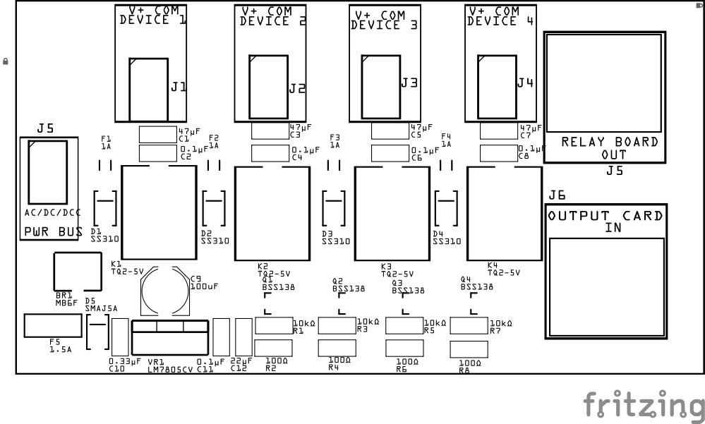
This section combines both the component specifications and the assembly instructions to ensure a smooth assembly process. Below is a comprehensive list of components, their placement on the PCB, and orientation details to assist you during assembly.
High-Level Steps for Assembly:
- PCB for the card can be ordered from any PCB fabricator using these Gerber Files.
- Clean PCB with alcohol to remove residue. See Cleaning_PCB for details.
- See also: Soldering Tips
- PCB Components - listing of components used for PCB assembly
- PCB Parts - listing of parts used for PCB assembly
![]()
![]()
| Component Identifier | Count | Type | Value | Package | Purpose | Orientation |
|---|---|---|---|---|---|---|
| Bridge Rectifiers | ||||||
| BR1 | 1 | Bridge Rectifier | MB6F | SOP-4 | Converts DCC pulsating AC-like waveform into a DC-like pulsating waveform for current detection. | Position IC’s indent to PCB left edge) |
| Capacitors | ||||||
| C1, C3, C5, C7 | 4 | Capacitor-Ceramic | 47uF | 1206 X7R | Used for surge buffering of relay coils | None |
| C2, C4, C6, C8 | 1 | Capacitor-Ceramic | 0.1uF | 1206 X7R | Used for high freq snubbing of relay coils | None |
| C9 | 1 | Capacitor-Polymer Solid | 100 µF | 6.3x5.8mm SMD | Used by 5V voltage regulator for input filtering. | Anode positioned toward PCB top edge |
| C10 | 1 | Capacitor-Ceramic | 0.33 uF | 1206 X7R | Used by 5V voltage regulator for input filtering. | None |
| C11 | 1 | Capacitor-Ceramic | 0.1uF | 1206 X7R | Used by 5V voltage regulator for output filtering. | None |
| C12 | 1 | Capacitor-Ceramic | 22 uF | 1206 SMD | Used by 5V voltage regulator for output filtering. | None |
| Diodes | ||||||
| D1 - D4 | 4 | Diode-Schottky | SS310 | SMA | Protects against flyback from relay coil | Position cathode end (white line) to PCB bottom edge |
| D5 | 1 | TVS Diode | SMAJ5A | SMA | Input line Transient Voltage Spike (TVS) protection | Position cathode end (white line) to PCB top edge |
| D5, D6 | 2 | Diode-Schottky | SS310 | SMA | Protects against reverse current | Position cathode end (white line) to PCB bottom edge |
| Fuses & Protection | ||||||
| F1 - F4 | 4 | Fuse-PTC Polymer | 1A, >5 VDC | 1206 SMD | Protects from sustained overcurrent conditions | None |
| F5 | 1 | Fuse-PTC Polymer | 1.5A, >5 VDC | JK30, PTH | Protects from sustained overcurrent conditions | None |
| Connectors | ||||||
| J1 - J4 | 4 | JST XH Socket or 2-Position Spring Terminal Connector | 2P, 2.54mm | PTH, vertical or horizontal | Connector to devices | Position connection outward |
| J5 | 1 | JST XH Socket or 2-Position Spring Terminal Connector | 2P, 2.54mm | PTH, vertical or horizontal | Connectors to layout power bus. | Position connection outward |
| J6 | 1 | RJ45 Socket | 8P8C | PTH | Connector to Output Card | Fits only one way |
| J7 | 1 | RJ45 Socket | 8P8C | PTH | Connect for daisy chaining a 2nd Relay Breakout Board | Fits only one way |
| Resistors | ||||||
| R1, R3, R5, R7 | 4 | Resistor | 10k Ω | 1206 SMD | Pullup for transistor gate | None |
| R2, R4, R6, R8 | 4 | Resistor | 100 Ω | 1206 SMD | Current limiting for transistor gate | None |
| Relays & Transistors | ||||||
| K1 - K4 | 4 | DPDT, TQ2-L-5V | 1A | DIP-10, PTH | Controls current to output devices | Position IC’s small dimple in corner (pin 1) towards PCB top edge |
| Q1 - Q4 | 4 | NPN Transistor | BSS138 | SOT-23, SMD | Sets relay on/off | Fits only one way |
| Voltage Regulators | ||||||
| VR1 | 1 | Voltage Regulator | LM7805CV | TO-220, SMD | Provides 5V to output device thru relay | Position heat sink towards PCB top edge |
Safety Precautions
- See Safety Precautions.
Testing and Verification
Visual Inspection
- Initial Check: Examine the board for any obvious issues like missing components, solder bridges, or components that are misaligned or not fully seated.
- Solder Joint Inspection: Use a magnifying glass or a microscope to inspect solder joints. Look for cold solder joints, insufficient or excessive solder, or any shorts between pads.
Functional Testing
Troubleshooting
- See I2C Trouble Shooting.
flowchart TD
  subgraph "Test Bench"
  	direction LR
    LED-Q{"Is the Power LED ON?"}
    PWR-Q{"Measure voltage <br>at PWR BUS (J9):<br><br>Is voltage >14 V?"}
    PWR-Q{"Measure input voltage at J5.<br><br>Is it >14 V (AC/DC)?"}
    Reg-In-Q{"Measure LM7805 <br>regulator input.<br><br>Is it >14V across pins 1/2?"}
    Reg-Out-Q{"Measure LM7805 <br>regulator output.<br><br>Is it ~5 V across pins 2/3?"}
    Input-Test-Q{"Apply 5 V to <br>each input line (J6).<br><br>Does corresponding device <br>turn on?"}
    Relay-Click-Q{"Did the relay click?"}
    Connector-Q{"Measure device connector <br>pins (J1-J4) voltage.<br><br>Is it ~5V across <br>each set of pins?"}
    Pass[" Relay Breakout Board <br>Passed Bench Test"]

    Fix-PWR["Low input voltage: <br>Fix input voltage or <br>replace power source"]
    Fix-Reg-Input["Low voltage to regulator: <br>Check fuse, <br>soldering, and traces"]
    Fix-Reg-Output["Bad regulator circuit: <br>Check regulator soldering or <br>replace LM7805"]
    Fix-Coil["Bad relay circuit: <br>Check diode (D1–D4), <br>fuse (F1–F4)"]
    Fix-Relay["Bad relay circuit: <br>Check relay contacts (COM–NO), <br>socket soldering, or <br>trace damage"]
    Fix-LED["Bad LED circuit: <br>Check LED and resistor"]
    Fix-Device["Bad output device: <br>Check device wiring, <br>polarity, and operation"]

    Start -- "Verify Power"--> LED-Q
    LED-Q -- "Yes, power LED is on" --> Input-Test-Q
    LED-Q -- "No, power LED off" --> PWR-Q
    Input-Test-Q -- "Yes, device turned on" --> Pass
    Input-Test-Q -- "No, device didn't turn on" --> Relay-Click-Q
    Relay-Click-Q -- "Yes, relay is working" --> Connector-Q
    Relay-Click-Q -- "No, relay didn't click" --> Fix-Coil
    Connector-Q -- "Yes, device connection <br>has power" --> Fix-Device
    Connector-Q -- "No, no power at connector" --> Fix-Relay
    PWR-Q -- "No, low input voltage" --> Fix-PWR
    PWR-Q -- "Yes, input voltage >14V" --> Reg-In-Q
    Reg-In-Q -- "No, low voltage to regulator" --> Fix-Reg-Input
    Reg-In-Q -- "Yes, regulator voltage input is good" --> Reg-Out-Q
    Reg-Out-Q -- "Yes, regulator output <br>voltage is ~5V" --> Fix-LED
    Reg-Out-Q -- "No, regulator output <br>voltage not ~5V" --> Fix-Reg-Output
  end
  %% Color classes
  classDef question fill:#d3d3d3,stroke:#333,stroke-width:2px,font-size:14px;
  classDef error fill:#FFA07A,stroke:#333,stroke-width:2px,font-size:14px;
  classDef success fill:#c6f6c6,stroke:#2c7a2c,stroke-width:2px,font-size:14px;

  class LED-Q,Relay-Click-Q,Device-On-Q,PWR-Q,Reg-In-Q,Reg-Out-Q,Input-Test-Q,Connector-Q question;
  class Fix-PWR,Fix-Reg-Input,Fix-Reg-Output,Fix-LED,Fix-Coil,Fix-Relay,Fix-Device error;
  class Start,Pass success;
Appendences
PCB Specifications
Specifications for the Relay Breakout Board include:
| Characteristic | Value |
|---|---|
| Max Output Devices | 4 |
| Max Breakout Boards Per Output Card | 4 |
| Output | 5 VDC @ 1A |
Here’s a rewritten How It Works for your relay breakout board with the updates we discussed (latching relays, Line 7/Line 8 usage, optional local regulator, and diode protection). I’ve kept the structure close to your original so it drops right into your docs:
How It Works
The Relay Breakout Board uses TQ2-L-5V single-coil latching relays, one per line, to switch each device’s COM line under control of the Output Card. Because the relays latch, coil current is only required briefly during a set/reset pulse.
Notes:
- In the following, the Output Card is used as the example control source. The same principles apply if the relay breakout board is driven by a Node Card I/O line or a Digital I/O Card.
- NoAlways set the LCC card’ LINE 8 jumper so Line 8 = GND. This ensures a common return for the MCP23017 signals, MOSFET drivers, and relay coils.
Device Control (per Line)
- Control Signal & MOSFET Driver
- Output Line n from the Output Card → 100 Ω gate resistor → BSS138 N-MOSFET gate.
- When Output Line n goes HIGH (3.3 VDC), the MOSFET conducts and sinks current through the selected relay coil (Coil− → Line 8 GND). Coil+ is tied to the +5 VDC rail.
- After the short pulse, the relay remains latched mechanically; no holding current is required.
- Contact Switching
- Each relay has one set of isolated contacts:
- COM → fused connection to the user’s device COM input
- NO/NC → selectable outputs (typically tied to layout bus or GND, depending on use)
- Set pulse → selected coil energized → relay toggles, COM tied to NO.
- Reset pulse → opposite coil energized → relay toggles back, COM tied to NC.
- Each relay has one set of isolated contacts:
- Common Power Rails
- Relay coil power is provided from a +5 VDC rail. There are two options for this 5 VDC supply:
- Line 7 (Output Card 5 VDC) → simple, light-duty option. Suitable since only one coil is normally pulsed at a time.
- Local 5 VDC regulator fed from the layout accessory bus (AC/DC/DCC through a bridge rectifier) → recommended for heavy relay usage or multiple boards.
- Both supply options are diode-OR’d using Schottky diodes, so either may be connected without risk of back-feeding.
- Line 8 always provides the breakout board’s GND plane, tying together:
- Relay coil− pins
- MOSFET sources
- Regulator GND (if fitted)
- Flyback diode returns
- Device COM return paths
- Relay coil power is provided from a +5 VDC rail. There are two options for this 5 VDC supply:
Independent Line Operation
- Each line operates independently:
- Output Line n drives MOSFET n → pulses Coil n → Relay n toggles → switches Device n COM between NO and NC.
- Because the relays are latching, no continuous current is drawn once a line is set/reset.
Typical Usage Example
- Set Device 1 ON
- Output Line 1 pulses HIGH → MOSFET 1 conducts → Relay 1 coil energized → COM₁–NO₁ closes → Device 1 COM connected to layout bus.
- Reset Device 1 OFF
- Output Line 1 (paired reset coil) pulses HIGH → opposite relay coil energized → COM₁–NC₁ closes → Device 1 disconnected.
- Operate Lines 2–4
- Repeat the same process independently on Output Lines 2–4.
Connections
The purpose of the Relay Breakout Board and its connectors is to facilitate quick and easy connections between the Output Card and the output devices.
| Component Designator | Connector Label | Connector Type | Connection Number | Description |
|---|---|---|---|---|
| J1 - J4 | DEVICE 1-4 | JST XH, Spring Terminal | VDC+, COM | Connection to output devices |
| J5 | PWR BUS | JST XH, Spring Terminal | AC/DC/DCC | Connection to layout power, regulated to 5V for controlling output devices |
| J6 | OUTPUT CARD | RJ45 Socket | 1 - 4 | Connects Output Card lines 1-4 to a device thru a relay. When 5V present, the relay is close and current flow thru the device. |
| J7 | RELAY BOARD | RJ45 Socket | 1-4 | Connects Output Card lines 5-8 to a daisy chained 2nd Relay Breakout Board which then controls 4 additional devices. |
PCB Protection
The Relay Breakout Board includes layered protection to guard against over‑current, inductive spikes, reverse transients and regulator instability. Below is the updated protection summary for your current design.
| Protected Element | Protection Component | Function | Specifications | Location |
|---|---|---|---|---|
| Board Input (5 VDC supply in) | JK30 1.5 A Polyfuse | Limits sustained over-current, auto-resettable | Hold: 1.5 A, Trip: ~3–4 A, PPTC | Between MB6F bridge output and LM7805 VIN |
| Dual 5 VDC Sources (Line 7 vs. Local Regulator) | Schottky Diodes (D6–D7, SS310) | Prevents back feeding between LCC card’s 5 VDC (Line 7) and local 5 VDC regulator | Vf ≈ 0.3–0.4 VDC @ 100 mA, 1–3 A IF, 40–100 VDC VR | Anode from each 5 VDC source, cathodes tied together to breakout +5 VDC rail |
| 5 VDC Bus (after regulation) | TVS Diode (D5, SMAJ5A) | Clamps high-voltage transients on the 5 VDC rail | 5 VDC standoff, ~6.4 VDC breakdown, ~8 VDC clamp, SMA package | Across 5 VDC → GND right at LM7805 VOUT pins |
| LM7805CV Regulator | Decoupling Capacitors | Ensures loop stability and filters high-frequency noise | 0.33 µF ceramic on VIN, 0.1 µF ceramic on VOUT, 100 µF bulk | As close as possible to VIN–GND and VOUT–GND pins on regulator |
| Each Relay Coil | Flyback Diode (D1–D4, SS310) | Absorbs inductive kick when coil de-energizes | Schottky, 3 A IF, 100 VDC VR, Vf ≈ 0.5 VDC | Across each coil: cathode to coil+, anode to coil– |
| Ceramic Capacitors (Added) | Reduces coil switching noise and EMI | 0.1 µF ceramic, 47 µF ceramic |
Across each relay coil terminals | |
| Individual Device Power Lines | Slow-blow Fuses (F1–F4) | Protects each device from sustained over-current | 1 A slow-blow (device-dependent) | In series with each device’s VDC+ input (J1–J4) |
Notes:
- The fast‑blow fuse at the board input stops large faults before they stress the regulator or copper.
- TVS D5 protects the entire 5 VDC net from external spikes and surges.
- Local flybacks (SS310) on each relay coil keep inductive energy out of the shared 5 VDC bus.
- Per‑device slow‑blow fuses isolate faults to individual loads, avoiding a full board shutdown on a single device failure.
- Proper capacitor placement at the LM7805 pins prevents oscillation and keeps your 5 VDC rail rock‑solid under load.
- 0.1 µF Ceramic Capacitor: suppress high-frequency switching noise (EMI) generated when the relay coil is energized or de-energized. This capacitor helps reduce voltage spikes and electrical noise that can propagate through your circuit.
- 47 µF Ceramic Capacitor: bulk decoupling capacitor across the coil, this larger capacitor helps absorb lower-frequency transients and smoothens voltage changes associated with coil switching, complementing the smaller capacitor.