Sensor Card Assembly Guide
Table of contents
Table of contents
Introduction
See the How to Use Assembly Guides for detailed instructions.
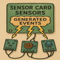
The Sensor Card is a flexible digital input card designed to support a wide variety of powered sensors that provide a logic-level output signal. It supplies power (selectable 3.3 V or 5 V), ground, and a signal return for up to six external sensors via a companion breakout board with standardized 3-pin (V/G/S) headers.
LCC Fusion uses the Digital Sensor Card to connect active sensors such as HTTM capacitive touch buttons, IR beam-break modules, Hall effect sensors, reed switches, and more. Each input line is monitored by the Node Card, which can be configured in firmware to generate LCC Events based on the digital signal state. These events can trigger layout automation, control signals, or initiate behavior in other LCC nodes.
The Sensor Card complements the Button Card (used for passive pushbuttons) and the Digital I/O Card (used for more general digital control). Its modular design, paired with the Sensor Breakout Board, makes it ideal for plug-and-play input integration from a wide variety of logic-based sensor modules.
Click  to listen to an audio explanation.
flowchart LR;
subgraph layout ["Train Layout"];
  direction LR;
  can["CAN Network"];
  sensor(("Digital Sensors (6x)"));
  sensorCard[["Sensor Card (12	x)"]]
  nodeCard["Node Card"];
  bb["Digital I/O <br>Breakout Board (2x)"];
  sensor --> |"Sensor<br/>(on/off)"|bb
  bb --> |"Digital Input <br/> (high/low)"|sensorCard
  sensorCard --> |"GPIO Output <br/> (high/low)"|nodeCard
  nodeCard --> |"LCC Event<br/>(on/off)"|can
end;
classDef lSalmonStyle fill:#FFA07A,stroke:#333,stroke-width:2px,font-size:18px;
class sensorCard lSalmonStyle;
classDef lightGrayStyle fill:#d3d3d3,stroke:#333,stroke-width:2px,font-size:22px;
class layout lightGrayStyle;
Assembly and Component Placement
This section combines both the component specifications and the assembly instructions to ensure a smooth assembly process. Below is a comprehensive list of components, their placement on the PCB, and orientation details to assist you during assembly.
High-Level Steps for Assembly:
- PCB for the card can be ordered from any PCB fabricator using these Gerber Files.
- Clean PCB with alcohol to remove residue. See Cleaning_PCB for details.
- See also: Soldering Tips
- PCB Components - listing of components used for PCB assembly
- PCB Parts - listing of parts used for PCB assembly
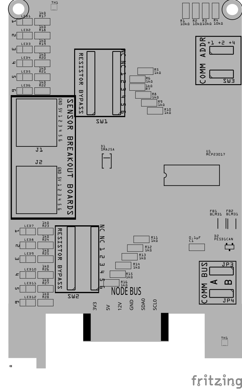
Below is a list of the PCB components used for this card (see diagram before reference):
![]()
![]()
| Component Identifier | Count | Type | Value | Package | Purpose | Orientation |
|---|---|---|---|---|---|---|
| Capacitors | ||||||
| C1, C2 | 2 | Capacitor-Ceramic | 0.1uF | 1206 X7R | Conditions/filters the current for the IC. | None |
| Diodes | ||||||
| D1 | 1 | TVS Diode | SMAJ5A | SMB SMD | Protects from high-voltage transients (>29 VDC). | Cathode end has a white line and positioned towards PCB left edge |
| D2 | 1 | ESD Diode | PESD1CAN | SOT-23 SMD | Provides I2C data bus electrostatic discharge (ESD) protection. | Fits only one way |
| LED1 - LED12 | 12 | LED | Red | 1206 SMD | Indicates when line goes LOW | Reference back of LED, position cathode towards PCB top edge |
| Filters & Noise Suppression | ||||||
| FB1, FB2 | 2 | Ferrite Bead | BLM31PG121SN1L | 1206 SMD | Suppresses noise on I2C data lines. | None |
| Connectors | ||||||
| J1, J2 | 2 | RJ45 Socket | 8P8C | PTH | Provides network cable (CAT5/6) connection to (1 or 2) Sensor Breakout Boards. | Fits only one way |
| Resistors | ||||||
| R25 | 1 | Resistor | 10kΩ | 1206 SMD | Current limiting for MCP23017 reset. | None |
| R26, R27, R28 | 3 | Resistor | 10kΩ | 1206 SMD | Limits current to SW1 and MCP23017 for the I2C address. | None |
| R13-R24 | 12 | Resistor | 1kΩ | 1206 SMD | Limits inrush current or transient voltage on input lines from external sensors. | None |
| R1-R12 | 12 | Resistor | 1kΩ | 1206 SMD | Current limiting for LED indicators | None |
| Selectors | ||||||
| JP1, JP2 | 2 | Male Header | 3P, 0.1” spacing | PTH | Used for COMM BUS selection (I2C hardware bus) for either BUS A or BUS B. | None |
| SH1, SH2 | 2 | Jumper Cap | 2.54mm | — | Used with I2C Bus and Vcc selections. Recommend tall caps for ease of use. | None |
| SW1 | 1 | DIP / Slide Switch | 3P, 2.54mm | PTH | Used for COMM ADDR selection (I2C address offset, 0-7). | Position ON towards PCB top. |
| ICs | ||||||
| U1 | 1 | I/O Expander (MCP23017 IC) | SSOP28 | SMD | Controls 12 GPIO pins using I2C serial interface. | Position indent on IC towards PCB bottom edge |
| U2 | 1 | EEPROM | AT24C02 | SOIC-8 | Memory for card’s type and description | IC indent is positioned towards PCB top edge |
Tools Required
For a list of recommended tools, refer to List of recommended tools.
Testing and Verification
Configure the BOD Card:
-
Select the
COMM BUSby positioning (2) Jumper Caps on eitherAorBmale header pins (JP1, JP2) -
Select the
COMM ADDRESSswitch (SW1) by sliding each of the 3 switches to either theONorOFFposition. Setting a switch to ON increments the address by 1, 2, or 4 for an address range of 0 to 7. Up to 8 devices can then be configured forAand 8 forB.
The following test and verifications of the card should be performed after a through inspection of the card’s soldering. Check all of the PTH component pins and SMD pads. Make sure there are no solder bridges between pins and pads.
Visual Inspection
-
Initial Check: Examine the board for any obvious issues like missing components, solder bridges, or components that are misaligned or not fully seated.
-
Solder Joint Inspection: Use a magnifying glass or a microscope to inspect solder joints. Look for cold solder joints, insufficient or excessive solder, or any shorts between pads.
-
Component Orientation: the IC’s are correctly oriented according to the PCB silkscreen or schematic.
Connectivity Testing
Continuity Check: Use a multimeter in continuity mode to check for shorts between power rails and ground, and to ensure there are no open circuits in critical connections.
Power-Up Tests
- Assembly a tested Power Module to the LCC Fusion Node Card.
- Apply Power to the Power Module and verify the following:
- Check for Hot Components: Feel for components that are overheating, which could indicate a problem like a short circuit or incorrect component.
Functional Testing
Functional testing of the card can be performed after completing the power-up testing. Testing consists of testing network communiations, followed by the sensing of current in a layout track block.
HW Communications Testing
Communications testing verifies the LCC Node can communicate with the BOD Card’s I2C IC via the Node Bus Hub connections. This is performed using the LCC Fusion Node Card’s testing firmware and a serial monitor.
-
Insert the BOD Card into a Node Bus Hub along with a LCC Fusion Node Card.
-
Install LCC Fusion Project firmware that includes serial monitor for testing.
-
Verify that the I2C connection between the LCC Fusion Node Card and the BOD Card work.
See Testing I2C Cards for details on how to test the communications for a I2C enabled card.
MCP IC Testing
After hardware communication has been established, to verify the MCP IC, use the Node’s serial monitor to simulate an input from each of card’s input pins as follows:
- In the serial monitor’s input, enter
Mfor the LCC Node’s serial monitor Main Menu. - Select
[1] Node Managementand[1] Device Testing Management - Select
[5] Simlulate MCP Device Input - From the list of MCP devices, select the device # for the BOD Card being tested
- Enter the number for the pin to tested.
- Using the JMRI LccPro event monitoring tool, verify the correct Event ID was issued.
Safety Precautions
- See Safety Precautions.
Provisioning the Card
- See Provisioning a Card.
Troubleshooting
- See I2C Trouble Shooting.
Appendences
PCB Specifications
![]()
| Characteristic | Value |
|---|---|
| Max Sensors | 12 |
| Sensor Voltage | 3v3 |
| Maximum Number of Cards per LCC Fusion Node Cluster | 161 |
- The LCC Fusion Node Cluster can support up to 16 cards, distributed across two I2C hardware buses, with a maximum of 8 cards per bus.
- Note: total includes all cards using the I2C address range of
0x20(MCP23017 IC).
- Note: total includes all cards using the I2C address range of
How It Works
The Sensor Card works by providing power (3.3 V or 5 V) and ground to external digital sensors, while monitoring the logic-level signal line (S) returned from each sensor through a 3-pin (V/G/S) connector on the Sensor Breakout Board.
Each signal line is routed to a I2C GPIO expander (MCP23017) and cabled to the Node Card, where it is configured in firmware as a digital input. The Node Card monitors the voltage state of each line and triggers LCC Events based on rising or falling signal transitions. This enables real-time layout automation responses to environmental or user input.
Sensors connected to the Digital Sensor Card typically drive their output line either HIGH (active) or LOW (active), depending on type. The Sensor Card supports both configurations by allowing firmware-based options for:
- Pull-up or no pull-up resistor
- Active-high or active-low event logic
Examples include:
- HTTM capacitive touch buttons, which drive the line HIGH when touched.
- IR beam-break sensors, which pull the line LOW when an object interrupts the beam.
- Hall effect switches or reed switches, which signal LOW when a magnetic field is detected.
This modular sensing system simplifies layout wiring and allows users to plug in a variety of sensors without reconfiguring core logic — all using a consistent 3-wire interface and a single breakout cable per Sensor Card.
PCB Protection
To ensure the reliable operation and longevity of the Sensor Card, several protection components have been integrated. These components safeguard the Sensor Card from overcurrent, voltage spikes, and electrical noise. Below is a brief overview of each protection element and its role:
![]()
| Protected Component | Protection Component | Function | Specifications | Location |
|---|---|---|---|---|
| MCP23017 GPIO | 1 kΩ Resistor | Limits inrush current or transient voltage on input lines from external sensors. | Value: 1 kΩ (slide-switch selectable) | In series between sensor signal line (S) and MCP23017 input |
| MCP23017 | Decoupling Capacitor 0.1 µF | Filters out high-frequency noise and transient voltage spikes from the power supply, ensuring a stable voltage for the MCP23017. | Value: 0.1 µF | Across Vcc and GND near the MCP23017 |
| I2C Lines from LCC Fusion Node Bus Hub | Ferrite Bead BLM31PG121SN1L | Provides high-frequency noise suppression on the I2C lines. | Impedance: 120 Ω at 100 MHz | In series with the SDA and SCL lines of the I2C bus |
| I2C Lines from LCC Fusion Node Bus Hub | ESD Protection Diode PESD1CAN | Protects the I2C lines from electrostatic discharge and voltage spikes. | Reverse Stand-off Voltage (Vr): 24 VDC Clamping Voltage (Vc): 40 VDC |
Across the SDA and SCL lines from the card’s edge connector to GND, near the MCP23017. |
| Node Bus Hub Power (5V+) | TVS Diode | Provides overvoltage protection to prevent damage from voltage spikes on the hub bus | Voltage clamp at specified level (e.g., 6V) | Across the 5V+ and GND power lines |
| LEDs | Current Limiting | Protects LEDs from current overload. | Value: 1kΩ | In series with LED |
References
I²C GPIO Mapping (Sensor Card)
The Sensor Card receives digital sensor signals from 3-wire active sensor modules. These typically output 5 V logic levels. The card supplies 5 V and GND via RJ45 and reads logic states from L3–L8 using the MCP23017.
| RJ45 Line | Function | MCP23017 Pin | GPIO Line | Direction | Pull-up | Logic Levels | Purpose | Notes |
|---|---|---|---|---|---|---|---|---|
| L1 | Sensor 1 In | GPA0 | GP0 | Input | Enabled | LOW = Active | Reads sensor 1 | Sensor pulls line LOW when triggered |
| L2 | Sensor 2 In | GPA1 | GP1 | Input | Enabled | LOW = Active | Reads sensor 2 | Sensor pulls line LOW when triggered |
| L3 | Sensor 3 In | GPA2 | GP2 | Input | Enabled | LOW = Active | Reads sensor 3 | Sensor pulls line LOW when triggered |
| L4 | Sensor 4 In | GPA3 | GP3 | Input | Enabled | LOW = Active | Reads sensor 4 | Sensor pulls line LOW when triggered |
| L5 | Sensor 5 In | GPA4 | GP4 | Input | Enabled | LOW = Active | Reads sensor 5 | Sensor pulls line LOW when triggered |
| L6 | Sensor 6 In | GPA5 | GP5 | Input | Enabled | LOW = Active | Reads sensor 6 | Sensor pulls line LOW when triggered |
| L7 | 5V | — | — | — | — | — | Power supply | 5 V supply for sensors |
| L8 | GND | — | — | — | — | — | Power ground | Shared GND for all sensors |