Signal Masts Breakout Board Assembly Guide
Table of contents
Table of contents
Introduction
The Signal Masts Breakout Board , used in tandem with the PWM Card, is designed to manage the operation of signaling mast lamps. In a standard LCC Fusion Node Cluster, this board connects to the signal mast lamps (typically LEDs), interfacing with a PWM Card to adjust signal aspects in response to LCC Events. These events are often generated by configured Logics and Conditions, which monitor variables such as track block occupancy, the status of other signal masts, and the positions of turnout points.
flowchart LR;
can["CAN Network"];
subgraph layout ["Train Layout"];
n["Node Card"];
pwm["PWM Card"];
direction LR;
can --> |"LCC Event <br/> (on/off/speed"| n;
n --> |"PWM Signal <br/> (on/off, brightness)"| pwm;
pwm --> |"PWM Signal <br/> (on/off, brightness)"| bb["Signal Masts <br/> Breakout Board (16x)"];
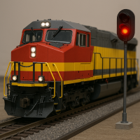
bb --> |"Lamp Control <br/>(on/off, brightness)"| m("Mast Signal Heads <br/> (8x 2-lamp, 5x 3-lamp)");
end;
classDef lSalmonStyle fill:#FFA07A,stroke:#333,stroke-width:2px,font-size:24px;
class bb lSalmonStyle;
classDef lightGrayStyle fill:#d3d3d3,stroke:#333,stroke-width:2px,font-size:24px;
class layout lightGrayStyle;
Assembly and Component Placement
This section combines both the component specifications and the assembly instructions to ensure a smooth assembly process. Below is a comprehensive list of components, their placement on the PCB, and orientation details to assist you during assembly.
High-Level Steps for Assembly:
- PCB for the card can be ordered from any PCB fabricator using these Gerber Files.
- Clean PCB with alcohol to remove residue. See Cleaning_PCB for details.
- See also: Soldering Tips
- PCB Components - listing of components used for PCB assembly
- PCB Parts - listing of parts used for PCB assembly
![]()
![]()
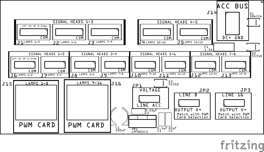
| Component Identifier | Count | Type | Value | Package | Required when using PWM Card VDC+ | Required when using ACC BUS VDC+ | Purpose | Orientation |
|---|---|---|---|---|---|---|---|---|
| Bridge Rectifiers | ||||||||
| BR1 | 1 | Bridge Rectifier | MB6F | SOP-4 | Optional | Required | Converts DCC pulsating AC-like waveform into a DC-like pulsating waveform for current detection. | Position IC’s indent to PCB left edge) |
| Capacitors | ||||||||
| C1 | 1 | Capacitor-Polymer Solid | 100 µF | 6.3x5.8mm SMD | Optional | Required | Used by 5V voltage regulator for input filtering. | Anode positioned toward PCB top edge |
| C2 | 1 | Capacitor-Ceramic | 0.33uF | 1206 X7R | Optional | Required | Used by 5V voltage regulator for input filtering. | None |
| C3 | 1 | Capacitor-Ceramic | 0.1uF | 1206 X7R | Optional | Required | Used by 5V voltage regulator for output filtering. | None |
| C4 | 1 | Capacitor-Ceramic | 22uF | 1206 X7R | Optional | Required | Used by 5V voltage regulator for output filtering. | None |
| Diodes | ||||||||
| D1, D2 | 2 | Diode-Schottky | SS310 | SMA | Required | Required | Protects against reverse polarity on PWR BUS DC+ and lines 7/15 | Cathode end has a white line and positioned towards PCB right edge |
| D3, D4 | 2 | Diode-Schottky | SS310 | SMA | Required | Required | Protects against reverse polarity on PWR BUS DC- and lines 8/16 | Cathode end has a white line and positioned towards PCB right edge |
| D5 | 1 | TVS Diode | SMAJ5A | SMA | Optional | Optional | GPIO pin Transient Voltage Spike (TVS) protection | Cathode end has a white line and positioned towards PCB right edge |
| Fuses & Protection | ||||||||
| F1 | 1 | Fuse-PTC Polymer | JK30, 1.5A, 16 VDC (or more) | 5.1mm pitch, PTH | Optional | Required | Protects from sustained overcurrent conditions, used by Crowbar diode for when reverse polarity occurs. | None |
| Connectors | ||||||||
| J1 - J5 | 5 | JST XH Socket | 4P, 2.54mm | PTH | Required when using 3-Lamp signals | Required when using 3-Lamp signals | Connectors to Mast 3-Lamp Head | Position connection outward from the PCB |
| J6 - J13 | 8 | JST XH Socket | 3P, 2.54mm | PTH | Required when using 2-Lamp signals | Required when using 2-Lamp signals | Connectors to Mast 2-Lamp Head | Position connection outward from the PCB |
| J14 | 1 | JST XH Socket or 2-Position Spring Terminal Connector | 2P, 2.54mm | PTH | Optional | Required | Connector to accessory bus (V+, GND) | None |
| J15, J16 | 2 | RJ45 Socket | 8P8C | PTH | Required | Required | Network cable (CAT5/6) connection from PWM Card. | None |
| Selectors | ||||||||
| JP1 | 1 | Male Header | 3-Pin | PTH | Required | Required | Use for selecting VDC+ for use with all LEDs (common Anode). | None |
| JP2, JP3 | 2 | Male Header | 3-Pin | PTH | Required | Required | Use for setting lines 8 and 16 to be either an outline line or VDC+ | None |
| SH1-SH3 | 3 | Jumper Cap (Shunt) | 2.54mm | - | Required | Required | Used for setting selections (JP1, JP2, JP3) | N/A |
| Voltage Regulators | ||||||||
| VR1 | 1 | Voltage Regulator | LM7805CV | PTH | Optional | Required | 5V voltage regulator for driving LEDs when VDC+ is configured for ACC BUS | Heat sink towards PC top edge |
Tools Required
Safety Precautions
- See Safety Precautions.
Testing and Verification
Visual Inspection
-
Initial Check: Examine the board for any obvious issues like missing components, solder bridges, or components that are misaligned or not fully seated.
-
Solder Joint Inspection: Use a magnifying glass or a microscope to inspect solder joints. Look for cold solder joints, insufficient or excessive solder, or any shorts between pads.
-
Use an Digital Multimeter (DMM) to test for continuity between the input connection pins and the output connection pins as follows:
Socket (Pin#) JST (Pin #) Socket (Pin#) JST (Pin #) J15 (1) J1 (1) and J6 (1) J16 (1) J3 (3) and J10 (1) J15 (2) J1 (2) and J6 (2) J16 (2) J4 (1) and J10 (2) J15 (3) J1 (3) and J7 (1) J16 (3) J4 (2) and J11 (1) J15 (4) J2 (1) and J7 (2) J16 (4) J4 (3) and J11 (2) J15 (5) J2 (2) and J8 (1) J16 (5) J5 (1) and J12 (1) J15 (6) J2 (3) and J8 (2) J16 (6) J5 (2) and J12 (2) J15 (7) J3 (1) and J9 (1) J16 (7) J5 (3) and J13 (1) J15 (8) J3 (2) and J9 (2) J16 (8) J13 (2) JP1 (1) J1 (3) JP2 (1) J14 (1) JP1 (2) J2 (2) JP2 (2) n/a JP1 (3) J5 (3) JP2 (3) JP14 (2)
Functional Testing
Refer to PWM Card for details on testing the BOD Card with the BOD Card.
Troubleshooting
- See I2C Trouble Shooting.
Appendences
PCB Specifications
Specifications for the BOD Card include:
| Characteristic | Value |
|---|---|
| Max Lamps | 15 |
| Max 3-Lamp Heads | 5 |
| Max 2-Lamp Heads | 8 |
| Max Total Current1 | 1000 mA |
| Maximum Signal Masts Breakout Boards per PWM Card | 1 |
- Max current with CAT6 23awg wiring. Signal Masts Breakout Board uses 48mil traces that support up to 3+A, allowing for more current across all output lines.
How It Works
The Signal Masts Breakout Board simply provides direct connections from the network cable inputs to the sockets that connect to signal lamps.
The Signal Masts Breakout Board is for use with LEDs that have a common Anode (V+) connection, witht their cathodes (GND) connected to each of the boards output lines.
Configuring Selections
There are three selectors that can be set as follows:
-
LED power (V+/GND) to be sourced from either the layout power bus or the PWM card (line 7/8 and 15/16).
-
LED connected to common cathode (GND) or anode (V+)
Note: Common cathode is most common wiring for LED sharing the same connection
| Selector Label | Components Indicator | Options | Description |
|---|---|---|---|
LINE 7LINE 15 |
JP1, JP3 | OUTPUT, V+ |
Configures lines 7 and 15 for either: - PWM mode: Functions like output lines 1 - 6. - PWR mode: Connects PWM Card’s GND to all lines for use with common cathode LEDs when LED COM is configured for GND (anode mode) (JP5) |
LINE 8LINE 16 |
JP2, JP4 | OUTPUT, V+ |
Configures lines 8 and 16 for either: - PWM mode: Functions like output lines 1 - 6. - PWR mode: Connects PWM Card’s 5V/12 VDC power to all lines for use with common anode LEDs when LED COM is configured for V+ (anode mode) (JP5) |
LED COM |
JP5 | GND, V+ |
Configures the COM source for all LEDs: - V+ (anode mode): LED common is sourced from either from:- PWM Card (via lines 7/15), configured as V+, or - layout DC+ power bus (via rectifier). - GND (cathode mode): LED common is sourced from either from:- PWM Card (via lines 8/16), configured as GND, or - layout DC- power bus (via rectifier). |
For Signaling details, refer to the PWM Card How it Works section.
PCB Protection
The Signal Masts Breakout Board includes several key protection mechanisms to safeguard both the board and the connected devices. Below is a detailed table outlining the protection provided against flyback voltage, reverse voltage, and current surges, ensuring the longevity and reliability of your setup.
| Protected Component | Protection Component | Function | Specifications | Location |
|---|---|---|---|---|
| Entire Board (Relays, Devices, Voltage Regulator) | Crowbar Diode, Resettable Fuse | Crowbar Protection protects against reverse polarity by short-circuiting the power supply when connected backward, blowing the fuse to protect the circuit | Diode becomes forward-biased if reverse polarity occurs | Across the power supply input (ACC VDC+ to ACC GND) C VDC+ to ACC GND) |
| Accessory Power (ACC VDC+) | TVS Diode | Provides overvoltage protection to prevent damage from voltage spikes on the accessory bus | Voltage clamp at specified level (e.g., 12 VDC) | Across the ACC VDC+ and ACC GND power lines |
Connections
The purpose of the Signal Masts Breakout Board and its connectors is to facilitate quick and easy connections between the LCC Fusion cards. For setups with requiring expansion, the Node Bus Hub provides connections to additional hubs.
| Component Designator | Connector Label | Connector Type | Connection Number | Description |
|---|---|---|---|---|
| J1, J2, J3, J4, J5 | LAMPS | JST XH 4P | 1 - 4 | Connection to 3 Lamps and their common connection |
| J6 - J13 | LAMPS | JST XH 3P | 1 - 3 | Connection to 2 Lamps and their common connection |
| J14 | ACC BUS | JST XH 2P, Terminal Connector | 1 - 2 | VDC+ and GND connection to layout accessory power bus (DC) |
| J15, J16 | NODE BUS | RJ45 Socket | 1 - 8 | Each pin connects to a lamp (LED). |