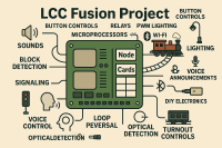
Node Card Assembly Guide
[TOC]
Table of contents
Table of contents
Introduction
See the How to Use Assembly Guides for detailed instructions.
In conjunction with the Node Bus Hub, the LCC Fusion Node Card provides an LCC compatible Node with ON/OFF control for up to 8 separate I/O devices. Typically, in an LCC Fusion Project LCC Fusion Node Cluster arrangement, there will be a Node Bus Hub, with one LCC Fusion Node Card, an optional I/O cards.
The LCC Fusion Node Card can be implemented with a number of optional features:
- Power Supply options (see Power Module for more details):
-
VIN: CAN serial connection via network cable (CAT5/6) or connectors (JST-XH or spring terminal).
VIN: 12 – 28 VDC DC via network cable (CAT5/6), USB-C-form socket, 5557 ATX connector, or DC-005 barrel jack.
- Accepts fixed-voltage laptop-style power supplies:
- 18 – 20 VDC DC at up to 3 A
- Either barrel plug (2.1 mm center-positive) or USB-C-form connector
- PD-compliant power supplies may also be used with a PD trigger/decoy module connected to the ATX-IN connector.
- This is a DC power input only – not a USB-C data or PD port.
- Do NOT connect directly to computers, phones, or PD chargers.
- Accepts fixed-voltage laptop-style power supplies:
-
-
Output Power:
- VOUT: 12 VDC - 28 VDC DC via 5557 ATX connection for powering other LCC Fusion Node Cards or Power-CAN Cards.
- VOUT: 5 VDC DC via USB-C for powering low voltage devices (e.g. RPI).
-
CANable adapter for Windows USB to CAN connection for JMRI integration.
-
CDI reset button (hold for 10 seconds to reset the CDI to factory setting)
-
Reset button to restart the Node.
-
LCC Fusion Node Bus Hub(RJ45) network cable connection to connect with a remote LCC Fusion Project Node Bus Hub
NOTES: LCC Node card provides serial output messages
- if Node Bus Hub voltages drop below their thresholds; 3V3, 5V, and 12V.
- if Node Card firmware when it detects the ESP32 NOT inserted into a Node Card (Node Card’s pin 0 provides a ‘signature’ voltage).
CAN Communications
The LCC Fusion Node Card connects to a CAN Network, enabling communication of LCC Events. It features two RJ45 sockets for easy in/out connections, allowing multiple Node Cards to be daisy-chained together. To simplify the network setup, the Node Card includes an auto-termination circuit, ensuring the correct 120 Ω termination is automatically applied to the last device in the chain, eliminating manual setup.
Below is a diagram illustrating the daisy-chaining of Node Cards via their RJ45 sockets with automatic CAN termination:
flowchart LR;
subgraph nodecard["Node Card (1)"];
direction LR;
esp32.1["ESP32"];
end;
subgraph nodecard2["Node Card (2)"];
direction LR;
autoterm2["CAN Auto-Termination (on)"]
esp32.2["ESP32"];
end;
can["CAN Network"];
can <-.-> |"Network Cable"| esp32.1;
esp32.1 <-.-> |"Network Cable"| esp32.2 <-.-> autoterm2;

classDef lSalmonStyle fill:#FFA07A,stroke:#333,stroke-width:2px,font-size:24px;
class nodecard,nodecard2 lSalmonStyle;
classDef lightGrayStyle fill:#d3d3d3,stroke:#333,stroke-width:2px,font-size:24px;
class can lightGrayStyle;
I2C Communication
The LCC Fusion Node Card supports I2C serial communication to interface with various I/O cards. Each device on the I2C bus is assigned a communication address and an address offset. The Node Card supports two I2C buses (Bus A and Bus B) with offsets ranging from 0 to 7.
Pullup resistors are used to “condition” the I2C lines (SDA and SCL), ensuring proper signal levels by pulling the lines to a high state when not actively driven. Conditioning of the I2C to maintain proper voltage levels is handled automatically.
Below is a diagram showing how I2C serial communication is used between the Node Card and multiple I/O cards:
flowchart LR;
subgraph nodebushub["Node Bus Hub"];
direction LR;
subgraph nodecard["Node Card"];
direction LR;
esp32["ESP32"];
end
card1["Digital I/O Card <br/> (MCP23017 IC)"];
card2["Digital I/O Card <br/> (PCA9685 IC)"];
card3["Digital I/O Card <br/> (ESP32 Module)"];
display["Display Monitor"];
storage["Micro-SD Card Reader"];
conditioning["I2C Conditioning"];
end
esp32 <-.-> |"I2C Serial <br/> (BUS A; ADDR 00)"| card1;
esp32 <-.-> |"I2C Serial <br/> (BUS A; ADDR 01)"| card2;
esp32 <-.-> |"I2C Serial <br/> (BUS B; ADDR 07)"| card3;
esp32 <-.-> |"I2C Serial <br/> (BUS A; ADDR xx)" | display;
esp32 <-.-> |"SPI" | storage;
card1 <--> device1["devices (16x)"];
card2 <--> device2["devices (16x)"];
card3 <--> device3["devices"];
classDef lSalmonStyle fill:#FFA07A,stroke:#333,stroke-width:2px,font-size:24px;
class nodecard lSalmonStyle;
classDef lightGrayStyle fill:#d3d3d3,stroke:#333,stroke-width:2px,font-size:24px;
class can lightGrayStyle;
I/O Connections
The LCC Fusion Node Card features an RJ45 socket for connecting up to 8 I/O devices, enabling direct interaction with a variety of peripherals. Supported I/O devices include:
- Touch pads
- LEDs
- Relays
- DC motors
- Buzzers
- Solenoids / Electromagnets
- Fans
Below is a diagram showing how a network cable is used to connect multiple I/O devices directly to the Node Card via its RJ45 socket:
flowchart LR;
can1["CAN Network"];
can2["CAN Network"];
n1["Node Card <br/>I/O ConnectionR<br>(RJ45)"];
n2["Node Card <br/>I/O Connection<br>(RJ45)"];
bb1[Digital I/O  Breakout Board];
bb2[Digital I/O  Breakout Board];

subgraph layout ["Node Card I/O Flow"];
direction LR;
idevice["Input Device (8x)"] --> |"Digital Input <br/>(high/low)"| bb1;
bb1 --> |"GPIO Input <br/> (high/low)"| n1;
idevice --> |"GPIO Input <br/> (high/low)"| n1;
n1 -.->|"LCC Event<br/>(on/off)"| can1;

can2 -.-> |"LCC Event<br/>(on/off)"|n2;
n2 --> bb2;
bb2 --> |"Digital Output<br/>(high/low)"| odevice["Output Device (8x)"];
n2 --> |"Digital Output <br/> (high/low)"| odevice;

end;
classDef lSalmonStyle fill:#FFA07A,stroke:#333,stroke-width:2px,font-size:24px;
class n1,n2 lSalmonStyle;
classDef lightGrayStyle fill:#d3d3d3,stroke:#333,stroke-width:2px,font-size:24px;
class layout lightGrayStyle;
Assembly-Configuration Options
The Node Card supports multiple assembly configurations to fit various use cases.
![]()
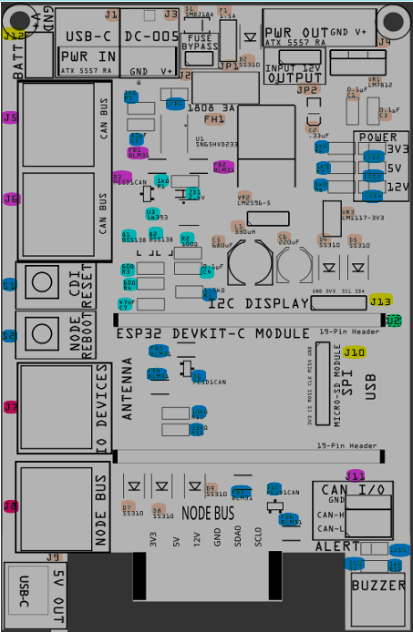
The PCB diagram shown above highlights different components based on their associated configuration. Each color-coded component corresponds to a specific configuration, which is further detailed in the table below.
To use this reference effectively:
- Match the Colors: Each assembly option in the table has a matching color in the PCB diagram. This helps identify which components are needed for a specific configuration.
- Locate Components Quickly: The highlighted component designators (e.g., D5, J1, JP1) on the PCB indicate where each part is placed.
- Identify Required vs. Optional Parts: The table differentiates between required components (essential for functionality) and optional components (enhancements or variations).
- Cross-Reference for Clarity: If you’re unsure about a part’s placement, use the designator labels on the PCB along with the descriptions in the table.
This approach ensures a clear, visual guide for assembling the Node Card based on your specific needs.
![]()
| Configuration | Required/Optional | Description | Required Components | Optional Components |
|---|---|---|---|---|
| ESP32 & I2C Support | Required | Provide ESP32 DevKit-C Module Support for Node | • ESP32 DevKit-C Headers (U1) • I2C Noise Filtering: Ferrite Beads FB3, FB4, FB5, FB6 |
I2C Bus Protection: Diode D6, D10 (for ESD protection on the I2C data bus) • Reboot Button (S1) • CDI Reset Button (S2) |
| CAN Termination Support | Required | I2C Low Voltage Detection and Correction | • Voltage Comparator (U3, ZD1, R1, R2) • 120$\Omega$ Switching Circuit R3, R4, C7, Q1, Q2) |
None |
| Power-Input | Required | Provides power input connectors with high-voltage transient protection and input filtering. | • TVS Protection: diode D1 • Reverse‑polarity Protection: diode D2 •Reverse Current Protection diodes D4, D5, D8 • Overcurrent Protection: Slow‑burn fuse F1 • 3A Fuse Holder: FH1 with 3A fuse |
• USB‑C Power In Socket (J1) • Wired Power In Connector J2 • DC‑005 Power In Connector (J3) |
| 3.3 VDC Output | Required | Supplies regulated 3.3 VDC to the Node Bus. | • 3.3 VDC Regulated Output (VR3) • Reverse Current Protection: Diode D7 |
None |
| 5 VDC Output | Required | Supplies regulated 5V to the Node Bus with proper filtering and protection. | • 5V Regulated Output: Buck regulator VR2 accompanied by filter capacitors C5 (100 µF). C2, C6 (100 µF), C4 (0.33 µF), C9 (1nF), C10 (0.1 µF), and , C11 (1 µF), inductor L1, voltage divider resistors R13 (3.3K$\Omega$) and R14 (1K$\Omega$) • Reverse/Output Protection: Diode D8 |
• 5V USB-C Output Connector (J9) |
| 12 VDC Output | Required | Provides regulated 12 VDC (or higher) for powering external devices and the LCC Fusion Node Bus Hub. | • 12 VDC Regulated Output: Voltage regulator VR1, capacitors C3 ( 0.1uF) and C2( 0.33uF) • Reverse/Output Protection: Schottky diodes D4, D5, D9 |
• 12 VDC Output Connectors: J4 (for 12 VDC @ 3A output) |
| CAT-Wired CAN BUS Option | Optional | Enables wired CAN Bus connectivity over CAT network cable, supporting data exchange with other LCC Fusion Nodes. | • Reverse Polarity Protection: Diode D10 (protects input power from CAN Bus connectors) • CAN Bus Noise Suppression: Ferrite beads FB1 and FB2 |
• CAN Bus Connections: RJ45 connectors J5 and/or J6 • ESD Protection: Diode D3 |
| Indicators and Controls Support Option | Optional | Setup for Power Indicators and Firmware Controls | • Power Indicators (LED2, LED3, LED4, R6, R7, R8) • Voltage Divider for 12 VDC Detection (R10, R11) |
• Blown Fuse Indicator (LED1, R9, C8) • Buzzer (SG1) • ALERT Indicator (LED5,R12) |
| Power Inputs | Optional | Setup for additional power inputs | • USB-C Connector (J1) • ATX 5557 Connector (J2) • DC-005 Connector (J3) |
None |
| Power Output | Optional | Setup for power additional Node Cards | • ATX 5557 Connector (J4) | |
| I/O Device Support Option | Optional | Setup for supporting I/O Devices (e.g., LEDs, buttons) through network cable. | • I/O Device Connector (J7) | None |
| Remote Node Bus Hub Support Option | Optional | Setup for connecting to a remote Node Bus Hub | • Network Cable Connection to remote Node Bus Hub (J8) | None |
| 5V Power Output | Optional | Setup for powering remote 5V devicde (e.g. RPI) | • USB-C Connector (J9) | |
| Increased File Storage Option | Optional | Setup for connecting Micro SD-Card Reader (use is TBD) | • SPI Connector (J10) | None |
| Display Monitor Option | Optional | Setup for connecting an I2C enabled display monitor | • I2C Connector (J13) | None |
| Battery Backup Support Option | Optional | Enables battery backup for increased system availability. | • Battery Connector (J14) | None |
| CANable Module Option, or CAN I/O | Optional | Supports connection of a 2/3-wired CANable module or CAN I/O for interfacing with a computer. | • CANable Isolated Module ** (J15) • CAN I/O (J15) |
None |
| Alert Buzzer | Optional | Support for alerts via buzzer | • 3V Buzzer (SG1) | None |
| CDI Reset | Optional | Support for resetting the CDI configuration to factory settings | • Tactile Button (S1) | None |
| Node Reboot | Optional | Support for rebooting the Node (ESP32) | • Tactile Button (S2) | None |
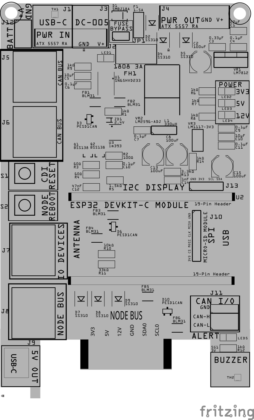
Assembly and Component Placement
This section combines both the component specifications and the assembly instructions to ensure a smooth assembly process. Below is a comprehensive list of components, their placement on the PCB, and orientation details to assist you during assembly.
High-Level Steps for Assembly:
- PCB for the card can be ordered from any PCB fabricator using these Gerber Files.
- Clean PCB with alcohol to remove residue. See Cleaning_PCB for details.
- See also: Soldering Tips
- PCB Components - listing of components used for PCB assembly
- PCB Parts - listing of parts used for PCB assembly
Below is a list of the PCB components used for this card (see diagram before reference):
![]()
![]()
| Component Identifier | Count | Type | Value | Package | Purpose | Orientation |
|---|---|---|---|---|---|---|
| Capacitors | ||||||
| C1 | 1 | Ceramic Capacitor | 22 uF | 1206 X7R | Used by 12V voltage regulator for input filtering | None |
| C2 | 1 | Polymer Capacitor | 100 µF | 6.3x5.8mm , SMD | Used by 12V voltage regulator for input filtering | Anode positioned toward PCB top edge |
| C3 | 1 | Ceramic Capacitor | 0.33 uF | 1206 X7R | Used by 12V voltage regulator for input filtering | None |
| C4 | 1 | Ceramic Capacitor | 0.1 uF | 1206 X7R | Used by 12V voltage regulator for output filtering | None |
| C5 | 1 | Ceramic Capacitor | 10 uF | 1206 X7R | Used by fuse circuit to cause slow LED fade in/out | None |
| C6 | 1 | Ceramic Capacitor | 0.1 uF | 1206 X7R | IC protection (U1) | None |
| C7 | 1 | Ceramic Capacitor | 0.1 uF | 1206 X7R | Used by 5V voltage regulator for input filtering | None |
| C8, C13 | 2 | Polymer Capacitor | 100 µF | 6.3x5.8mm , SMD | Used by 5V voltage regulator for input/output filtering | Anode positioned toward PCB top edge |
| C9 | 1 | Ceramic Capacitor | 0.1 uF | 1206 X7R | Used by 3V3 voltage regulator for input filtering | None |
| C10 | 1 | Ceramic Capacitor | 10 uF | 1206 X7R | Used by 3V3 voltage regulator for input filtering | None |
| C11 | 1 | Capacitor-Ceramic | 0.1uF | 1206 X7R | Used by 3V3 voltage regulator for output filtering | None |
| C12 | 1 | Ceramic Capacitor | 47 uF | 1206 X7R | CAN termination circuit | None |
| C14 | 1 | Capacitor-Ceramic | 1n F | 1206 X7R | Shunts LM2596S-ADJ output high freq spikes | None |
| C15 | 1 | Polymer Capacitor | 100 µF | 6.3x5.8mm , SMD | Used by 3V3 voltage regulator for output filtering | Anode positioned toward PCB top edge |
| Diodes | ||||||
| D1 | 1 | TVS Diode | SMBJ18A | SMB SMD | Protects from high-voltage transients (>29 VDC) | Cathode end has a white line and positioned towards PCB right edge |
| D2, D4, D5, D7, D8, D9 | 6 | Schottky Diode | SS310 | SMA | Reverse polarity and current protection | Cathode end has a white line and positioned towards PCB bottom edge |
| D3, D6, D10 | 3 | ESD Diode | PESD1CAN | SOT-23 SMD | I2C data bus ESD protection | Fits only one way |
| ZD1 | 1 | Zener Diode | 2.4 VDC | BZT52 | 2.4 VDC reference voltage | Cathode end has a white line and positioned towards PCB right edge |
| Fuses & Protection | ||||||
| FH1 | 1 | Fuse Holder | 1808 with 3A | SMD | Protects from sustained overcurrent conditions | None |
| F1 | 1 | PTC Polymer Fuse | JK30, 1.5A, 16 VDC (or more) | 5.1mm pitch, PTH | Overcurrent protection | None |
| Filters & Noise Suppression | ||||||
| FB1, FB2 | 2 | Ferrite Bead | BLM31PG121SN1L | 1206 SMD | CAN Network Bus Data Line Noise Suppression Ferrite Bead | None |
| FB3, FB4 | 2 | Ferrite Bead | BLM31PG121SN1L | 1206 SMD | I2C Data Line Noise Suppression Ferrite Bead | None |
| Connectors | ||||||
| J1 | 1 | USB-C Socket | 4-Pin | SMD | Power input connector to power the LCC Fusion Node Card when power is not being supplied via the CAN Network Bus network cable | Fits only one way |
| J2 | 1 | Connector | 5557 ATX RA | PTH | Power input connector to power the LCC Fusion Node Card when power is not being supplied via the CAN Network Bus network cable | GND pin is marked on board with square pad |
| J3 | 1 | Power Jack | DC-005 | PTH | Power input connector to power the LCC Fusion Node Card when power is not being supplied via the CAN Network Bus network cable | Fits only one way |
| J4 | 1 | Connector | 5557 ATX RA | PTH | Power input connector to power the LCC Fusion Node Card when power is not being supplied via the CAN Network Bus network cable | GND pin is marked on board with square pad |
| J5-J8 | 4 | RJ45 Socket | 8P8C | PTH | CAN Bus and I/O networking | Fits only one way |
| J9 | 1 | USB-C Socket | 4-Pin | SMD | Power output connector for external devices | Fits only one way |
| J10 | 1 | Header | 6-Pin Male | PTH | Mounting for Micro-SD Reader Module | None |
| J11-J12 | 2 | Female Headers | 19-Pin | PTH | Mounting for ESP32 DevKit-C module | None |
| J13 | 1 | Female Headers | 4-Pin | PTH | Mounting for I2C LCD | None |
| J14 | 1 | JST XH Socket or 2-Position Spring Terminal Connector | 2P, 2.54mm | PTH, vertical or horizontalPTH | Mounting battery connector | See silkscreen |
| J15 | 1 | JST XH Socket or 2-Position Spring Terminal Connector | 3P, 2.54mm | PTH, vertical or horizontalPTH | Mounting of a CANable Isolated Module or CAN I/O | None |
| Selectors | ||||||
| JP1 | 1 | Male Header | 3-Pin, 2.54mm | PTH | Used to bypass the fast blow fuse when not desired | None |
| SH1 | 1 | Jumper Cap | 2.54mm | — | Used with JP1 | None |
| Inductors & Resistors | ||||||
| L1 | 1 | Inductor | 33uH | 8x10mm, PTH | Used for 5V voltage regulation | None |
| R1 | 1 | Resistor | 1k Ω | 1206 SMD | Current limiting for reference voltage | None |
| R2 | 1 | Resistor | 100 Ω | 1206 SMD | Low Pass Filter for low signal detection | None |
| R3, R4 | 2 | Resistor | 60 Ω | 1206 SMD | CAN termination circuit | None |
| R5 | 1 | Resistor | 1.5k Ω | 1206 SMD | Part of CDI Factory Reset circuit | None |
| R6-R9, R12 | 5 | Resistor | 1k Ω | 1206 SMD | Current limiting for power output and alerts LEDs | None |
| R13 | 1 | Resistor | 3.3k Ω | 1206 SMD | Regulator voltage divider (R2) damping lower freq. | None |
| R14 | 1 | Resistor | 1k Ω | 1206 SMD | Regulator voltage divider (R1) | None |
| R15-R18 | 4 | Resistor | 47 Ω | 1206 SMD | Edge damping of I2C data lines | None |
| R19, R20 | 2 | Resistor | 47 Ω | 1206 SMD | Edge damping of CAN bus lines | None |
| R22, R24 | 2 | Resistor | 10k Ω | 1206 SMD | Voltage Divider (high end) | None |
| R23 | 1 | Resistor | 5.6k Ω | 1206 SMD | Voltage Divider (low end) for HW ID check | None |
| R21 | 1 | Resistor | 20k Ω | 1206 SMD | Voltage Divider (low end) for 5 VDC low detection | None |
| R25 - R32 | 8 | Resistor | 1k Ω | 1206 SMD | Current limiting for I/O lines | None |
| Switches & Indicators | ||||||
| LED1-LED5 | 5 | LEDs | Red/Green | 1206 SMD | Status and alert indicators | Reference back of LED, position cathode towards PCB left edge |
| S1, S2 | 2 | Tact Button Switch | N/A | SMD | Factory reset or reboot buttons | Fits only one way |
| SG1 | 1 | Buzzer | 3V | Piezo Active Buzzer, 9650-5 VDC, SMD | Buzzer for firmware generated error/warning alerts | None |
| Transistors | ||||||
| Q1, Q2 | 2 | NPN Transistor | BSS138 | SOT-23, SMD | Sets relay on/off | Fits only one way |
| ICs | ||||||
| U1 | 1 | CAN Transceiver | SN65HVD233DR | SMD | CAN Communications | Package has small dimple in corner (pin 1) which is position to PCB top/right edges |
| U2 | 1 | MCU (Processor) | ESP32 DevKitC-V4 Module /w ESP32-WROOM-32D 4MB | PTH, 38-Pin wide | Main processor for Node Card | Position ESP32 development board’s USB connector to PCB right edge |
| U3 | 1 | Voltage Comparator | LM393 or LM2903N | SO-8, SMD | Detects low voltage in I2C lines | Package has small dimple in corner (pin 1) which is position to PCB top/left edges |
| Voltage Regulators | ||||||
| VR1 | 1 | Voltage Regulator | L7812CV | TO-220 PTH | 12 VDC regulator for Node Bus Hub | Heat sink towards top of board |
| VR2 | 1 | Voltage Regulator | LM2596S-ADJ | SMD | 5V regulator for ESP32 & Node Bus Hub | Fits only one way |
| VR3 | 1 | Voltage Regulator | LM1117-3V3 IC | SMD | 3.3 VDC regulator for Node Bus Hub | Fits only one way |
Step-By-Step Assembly
Testing and Validation
Safety Precautions
- See Safety Precautions.
Troubleshooting
- See I2C Trouble Shooting.
Appendences
Circuits Overview
Below is a high-level Circuits overview for the LCC Fusion Node Card, summarizing its key functional blocks. This table helps quickly identify each circuit’s purpose, providing a concise reference during assembly, configuration, testing, or troubleshooting of the Node Card.
| Circuit Name | Brief Description |
|---|---|
| Power Supply Circuit | Provides regulated power input/output options (3.3V, 5V, and 12V) with protection features including fuses, diodes, and regulators (L7812, LM2596, LM1117). |
| CAN Communication Circuit | Manages CAN network communication with automatic termination, includes CAN transceiver (SN65HVD233) and RJ45 connections for daisy-chaining nodes. |
| I²C Communication Circuit | Supports two separate I²C buses for communication with peripheral I/O cards, featuring noise filtering and ESD protection. |
| I/O Device Circuit | Allows connection and control of up to 8 I/O devices (digital, ADC, PWM, touch sensors) via an RJ45 socket. |
| ESP32 Microcontroller Circuit | Hosts the ESP32 DevKit-C module as the main processor, managing logic, device control, and communications on the Node Card. |
| SPI Circuit | Provides connectivity for SPI-based devices like Micro-SD Card readers for local storage. |
| Battery Backup Circuit | Optional support for connecting a backup battery, ensuring uninterrupted power supply to the Node Card. |
| USB Power Circuit | USB-C connections for input and output power (5V) to external devices (e.g., Raspberry Pi). |
| Protection Circuit | Comprehensive protection including reverse-polarity, reverse-current, overcurrent (fuses, polyfuses), transient voltage suppression (TVS diode), and electrostatic discharge (ESD diodes). |
| Indicators and Controls Circuit | LED indicators for power and fuse status, buzzer alerts for firmware-generated warnings/errors, and tactile switches for rebooting/resetting configurations. |
| Display Monitor Circuit | Optional I²C-based connection for an external display module to provide visual feedback or status monitoring. |
| Remote Node Bus Hub Circuit | RJ45 connector for extending Node Card connectivity to remote Node Bus Hubs for broader system integration. |
| Low Voltage Detection Circuit | Monitors Node Bus Hub power lines (3.3V, 5V, 12V) to detect and alert on voltage drops, preventing brownouts and ensuring stable system operation. |
| Hardware Identification Circuit | Identifies the hardware configuration or type of Node Card via ADC voltage readings, enabling automated hardware verification and configuration. |
PCB Specifications
Specifications for the Power-CAN Card include:
When using multiple Node Cards or Quad-Node Cards, consider using ATX, terminal, or DC-005 barrel connector to provide 5V @ 3A to the Node Bus Hub.
![]()
| Characteristic | Value |
|---|---|
| I/O Lines: (direct connection to devices, Node Analog Sensor Breakout Board, or Digital Sensor Breakout Board) | 6 (I/O line 7 = 5V, line 8=GND) |
| Nodes: Max number of Nodes (assuming 100 mA avg per Node ESP32) | 30 |
| Node Cards: Max number of Node Cards per Node Cluster | 21 |
| Input: Max supply voltage (limit of TVS Diode, SMBJ18 VDC) | 28 VDC |
| Input: Max supply current via CAN Bus network cable (limited by network cable’s 2 combined power wires) | 1.2A |
| Input: Max supply current via ATX 5557, Spring/Screw Terminal Connector, or DC-005 connector | 3A |
| Input: Max supply current USB-C connector | 2A |
| Output: Max 3V3 output current (LM1117-3V3 regulator limitation) | 800 mA |
| Output: Max supply current to output ATX 5557 or Spring/Screw Terminal connectors | 3A |
| Output: Max 5V output current to Node Bus Hub | 3A2,3 |
| Output: Max 12 VDC to the Node Bus Hub (L7812 regulator limitation) | 1.5A4,5 |
| Output: Max output current via USB-C | 2A |
| Output: Max output voltage to ATX 5557 or Spring/Screw Terminal Connector | Input Voltage minus ~0.4 - 1.7 VDC6 |
- Limit of Node Bus Hub (3A) within the Node Cluster (one or more Node Bus Hubs connected together via pin headers)
- The LM2596-ADJ switching regulator has a maximum current rating of 5A, but the output is limited to 3A due to:
- PCB traces (54 mil width), Vias (0.6mm holes), Diodes (SS310), and
- 3A polyfuse (resettable).
- The 5V switching regulator (LM2596-ADJ) operates with approximately a 10% efficiency loss, meaning the input current may exceed the output current by this margin.
- Limit of 1.5A by 12 VDC voltage regulator (L7812CV).
- The 12 VDC linear regulator (L7812) dissipates power as heat, resulting in an efficiency of around 85% (or ~15% efficiency loss), meaning the input current may exceed the output current by this margin.
- Voltage drop is caused by reverse voltage protection (two SS310 diodes in series)
Below is an updated version of your Node Card documentation with an additional Indicators & Additional Features section covering the requested items.
How It Works
The Node Card supports both power distribution and CAN network connectivity across LCC Fusion devices. It connects to the Node Bus Hub and enables stable power and reliable communication between multiple Node Cards and I/O modules. Key protections against network fluctuations and reverse voltage are built in.
CAN Network
The Node Card includes connections to the CAN Network for communications with other LCC protocol–enabled devices. Both network cable or 2/3-wire connections are supported.
The 2/3-wire connection could be use to connect with other LCC CAN enabled devices or to a (isolated) CANable Module connected to a computer for use with JMRI.
Correct termination of the CAN network is essential for reliable data transmission. To meet this, the Node Card and Quad-Node Card support auto-termination by detecting low voltage on the CAN network and applying a 120 Ω pullup resistor as needed.
Power Supplied to Local and Remote Node Bus Hubs
The Node Card provides regulated power to both local and remove Node Bus Hubs, with various connection and regulation options.
Remote Node Bus Hub: In addition to using the Node Card’s Node Bus (edge) connection to a Node Bus Hub, you can also link the Node Card to a separate (remote) Node Bus Hub for extended network coverage using a network cable.
- The L7812CV regulator converts the supply voltage to 12 VDC for use by both the Node Card and the Node Bus Hub.
- A LM2596-ADJ switching regulator provides a steady 5 VDC supply for the Node Bus Hub.
- A LM1117-3V3 linear regulator supplies 3.3 VDC to the Hub, meeting the lower voltage requirements of certain modules.
- Overcurrent protection is provided by two resettable polyfuses rated at 1.5A and 3A.
- Reverse polarity protection is included via a diode across all input lines.
- Reverse current protection is included via diodes on each output line.
- Noise filtering is implemented with capacitors on both input and output lines to stabilize and clean the power signal.
Multiple Power Inputs/Outputs are supported via voltage regulators:
- 5 VDC USB-C (input or output)
- 12 VDC output
- Power input via CAN bus network cable, ATX connection, or USB-C cable. Input power overload is protected using both slow and fast-blow fuses. A fuse holder allows the replacement of fast-blow fuse, which can also be bypassed using a Jump Cap.
- Battery Backup: An optional Battery Card can provide uninterrupted power, letting the Node Card continue operation if the main supply is lost.
This modular design also supports adding multiple Node Cards to a single Node Bus Hub to expand both power capacity and CAN connectivity, enabling flexible scaling for complex automation configurations.
Indicators & Additional Features
- Power Indicators: Onboard LEDs for 3.3 VDC, 5 VDC, and 12 VDC rails let you quickly verify that each voltage is active and within spec. A blown fuse indicator circuit also provides a visual alert if a the fast-blow fuse trips.
- Alert Buzzer & LED: Firmware can drive a buzzer and an additional LED to signal warnings or errors. The number of buzzes or LED blinks can be used as a diagnostic code for troubleshooting.
- CDI Reset & Node Reboot: The Node Card firmware supports the use of the Node Card’s tactile buttons for triggering a CDI parameter reset or rebooting connected devices, ensuring you can remotely recover or reconfigure nodes if needed.
- I/O Devices: the ESP32 supports connecting analog, digital, touch, and PWM devices such ase sensors, actuators, or other I/O modules for local or distributed automation tasks.
Connections
| Component Designator | Connector Label | Connector Type | Connection Number | Function | Description |
|---|---|---|---|---|---|
| NODE BUS | Card Edge | 1-12 | Power, Communications | Connection to Node Bus Hub | |
| J1 | PWR IN | USB-C1 | VDC+, GND | Power In | Connection from Power Supply (14-28 VDC, 0.5-3A) |
| J2 | PWR IN | ATX 5557 RA2 | VDC+, GND | Power In | Connection from Power Supply (14-28 VDC, 0.5-3A) |
| J3 | PWR IN | DC-0051 | VDC+, GND | Power In | Connection from Power Supply (14-28 VDC, 0.5-3A) |
| J4 | PWR OUT | ATX 5557 RA | VDC+, GND | Power In | Connection to next Power-CAN Card, or Node Card (14-28 VDC, 0.5-3A) |
| J5, J6 | CAN BUS | RJ45 Socket | 1-8; CAN-H, CAN-L, GND, undef, undef, GND, GND, VDC+ | Power & CAN In/Out | Connection to/from other LCC Nodes. Pin 1 pad is square (left side, front row). |
| J7 | I/O | RJ45 Socket | 1-8 | I/O (Digital, ADC, Touch, PWM) | Connection to input / output devices, or LCC Fusion breakout boards |
| J8 | NODE BUS | RJ45 Socket3 | 1-8; 3V3, 5V, 12 VDC, GND, SDA0, SCL0, SCL1, SDA1 | LCC Fusion Node Bus connection | Connection to LCC Fusion Node Bus Hub |
| J9 | 5 VDC OUT | USB-C | 5V, GND | Power Out | Connection to 5V devices (e.g. RPI) |
| J10 | SPI / MICRO-SD MODULE | 6-Pin Header | SPI (3V3, CS, MOSI, CLK, MISO, GND) | SD Card Reader | Used for local storage |
| J11-J12 | ESP32 | 19-Pin Header | 1-38 | ESP32 DevKit-C Socket | MCU for firmware |
| J13 | CAN I/O4, 5 | 3-Pin Header | CAN (GND, CAN-H, CAN-L) | CANable Device/Adapter, CAN Network | Used to connect to the CAN Network |
| J14 | BATT IN | 2P JST XH, screw/spring terminal | 12 VDC, GND | Battery Card | Connection to LCC Fusion Battery Card for power backup |
- Recommend a laptop power supply with a USB-C and DC-005 connectors with typically provide 18-20 VDC and >3A (>65W) for less than $20 on Amazon.
- Recommend using train layout accessory bus which is typically >12 VDC. If installed, replaces USB-C (J1) and DC-005 (J3) connections.
- Typically used to connected to a remote Node Bus Hub (board) as an alternative to using the NODE BUS edge connection to directly connect to a local Node Bus Hub. Pin 1 pad is square (left side, front row).
- Provides an alternative method of connect to the CAN Network. A CANable adapters attach to computers via USB.
- This connection does NOT provide a galvanic isolation link to the CAN Network for a electrical isolation between the CAN Network and LCC Fusion devices. For protection, insure that the CANable Adapter provides the required isolation.
PCB Protection
The LCC Fusion Node Card is equipped with several protection components to ensure reliable operation and safeguard against electrical faults. Below is an overview of each protection element integrated into the LCC Fusion Node Card and its role:
Here’s the updated row for low voltage detection, noting the minute-based alerts triggered until a reboot:
![]()
| Protected Component | Protection Component | Function | Specifications | Location |
|---|---|---|---|---|
| Entire Board (Relays, Devices, Voltage Regulator) | Crowbar Diode, Resettable Fuse | Crowbar Protection protects against reverse polarity by short-circuiting the power supply when connected backward, blowing the fuse to protect the circuit | Diode becomes forward-biased if reverse polarity occurs | Across the power supply input (ACC VDC+ to ACC GND) C VDC+ to ACC GND) |
| Entire Board (ESP32, Devices) | Low Voltage Detection Circuit | Monitors 3.3 VDC, 5V, and 12 VDC for voltage drops below their thresholds, triggering an alert message and buzzer every minute until reboot to prevent brownout conditions that may cause instability | Voltage threshold set to 3.0 VDC | ADC pin connected to the 3.3 VDC output from onboard regulator |
| Entire Power-CAN Card | Fast Blow Fuse | Protects from current overflow | Hold Current: 3A | In series with the incoming Vcc line |
| Entire Power-CAN Card | TVS Diode SMBJ18A | Protects from high-voltage transients by clamping voltage spikes, pthem from reaching sensitive components. | Stand-off Voltage: 28 VDC Clamping Voltage: 29.2 VDC |
Across the incoming Vcc and GND lines |
| CAN Bus | Automatic Termination | Provides proper termination to prevent signal reflections on the CAN bus. | Value: 2x 60 Ωs in series (120 Ωs) | Across CANH and CANL lines, automatically applied based on CAN network voltage while using a low-pass filter to measure peak voltage. |
| CAN Bus | ESD Protection Diode PESD1CAN | Protects the CAN bus lines from electrostatic discharge and voltage spikes. | Reverse Stand-off Voltage (Vr): 24 VDC Clamping Voltage (Vc): 40 VDC |
Across CANH to GND and CANL to GND |
| CAN Bus Line | Series Damping Resistor | Slows edge-rates and dampens reflections on long CAN bus runs (>100 mm), improving signal integrity. | Value: 47 Ω (1206) | In series with CAN lines at the SN65HVD233DR transceiver pins |
| I2C Bus Line | Series Damping Resistor | Slows edge-rates and dampens reflections on long I²C runs (>100 mm), improving signal integrity. | Value: 47 Ω (1206) | In series with SDA and SCL at the ESP32’s I2C pins |
| I2C Bus (each set) | ESD Protection Diode PESD1CAN | Protects the CAN bus lines from electrostatic discharge and voltage spikes. | Reverse Stand-off Voltage (Vr): 24 VDC Clamping Voltage (Vc): 40 VDC |
Across CANH to GND and CANL to GND |
| CAN Bus | BLM31PG121SN1L Ferrite Beads | CAN Network Bus Data Line Noise Suppression Ferrite Bead | In series with the CAN network lines | |
| I2C Bus (each set) | BLM31PG121SN1L Ferrite Beads | CAN Network Bus Data Line Noise Suppression Ferrite Bead | In series with the I2C network lines | |
| ESP32 Vcc | Decoupling Capacitor | Filters out high-frequency noise and transient voltage spikes from the power supply, ensuring stable voltage for the ESP32. | Value: 0.1 µF, 10uF ceramic | Integrated into DevKit-C Board |
| LM2596-ADJ Regulator | Output Capacitor | Filters out high-frequency noise and transient voltage spikes from the output, ensuring stable 5V regulation. | Value: 680 µF electrolytic | Across the output (5 VDC) and GND |
| L7812CV Regulator | Output Capacitor | Filters out high-frequency noise and transient voltage spikes from the output, ensuring stable 12 VDC regulation. | Value: 10 µF ceramic | Across the output (12 VDC) and GND |
| Ground Bus | 48mil Ground Bus | Provides a low-resistance path for all protection components, ensuring effective grounding and noise suppression. | Width: 48 mil | Used by all protection components |
Summary
These protection components work together to safeguard the LCC Fusion Node Card from various electrical faults. The CAN termination resistor ensures proper signal integrity on the CAN bus, while the ESD protection diodes protect the CAN bus and I2C lines from voltage spikes and electrostatic discharge. The decoupling capacitor filters out noise and transient voltage spikes, ensuring stable power for the ESP32. The ferrite bead suppresses high-frequency noise on the I2C lines. The input Vcc is protected by the Power Module, which includes a polyfuse and TVS diode for overcurrent and overvoltage protection. Together, these components ensure the LCC Fusion Node Card operates reliably in a potentially harsh electrical environment.
Flow of current
  flowchart TD;
  powerout["POWER OUTPUT <br/>(Input Power @3A)<br/> (ATX 5557)"];
  cannetwork["CAN Network"];
  subgraph nodecard ["LCC Fusion Node Card"];
 	  subgraph powerinput ["Power Supply Input Connectors"];
 		  direction LR;
      canbus["CAN BUS <br/> (Network Cable, RJ45 Socket)"];
      usb["USB </br> (USB-C Cable, USB-C Connector)"];
      atx["ACC BUS, or </br> Node Card <br/> (2x wires, ATX 5557 Socket)"];
      battery["Battery <br/> (2x wires, JST XH Socket)"];
    end;
    subgraph piprotection ["Input Protection"];
    	canbus --> |"1.5A, >14 VDC"| fuse3a["Fuse </br> Fuse Hold with fast blow <br/> (1808 3A )"];
    	usb --> |"3A, >14 VDC"| fuse3a;
    	atx --> |"3A, >14 VDC"| fuse3a;
    	battery --> |"12.6 VDC"| fuse3a;
      fuse3a --> tvs["TVS Diode </br> (SMBJ18A)"];
      tvs --> fuse1.5a["Fuse </br> Resettable <br/> (1.5A)"];
      fuse1.5a --> crowbar["Reverse Polarity <br/> Crowbar Diode <br/> (SS310)"];
      cannetwork --> esd["Electrostatic Discharge Protection (ESD)<br/> (PESD1CAN)"];
    end;
    subgraph regulators ["Power Output Voltage Regulators"];
      crowbar --> vs["Voltage Selector <br/> (12 VDC, or >14 VDC)"];
      vs -->  regulator12V["Voltage Regulator <br/>(LM7812, 12 VDC @1.5A)"];
      crowbar --> regulator5V["Voltage Regulator <br/> (LM2596-5, 5V @3A)"];
      regulator5V --> regulator3V3["Voltage Regulator <br/> (LM1117-3 VDC, 3V3 @1.5A)"];
      subgraph diodes ["Reverse Current Protection <br/> (SS310 (5x))"];
    	end;
  	end;
    regulator5V -->  |"5 VDC"| diodes;
    regulator3V3 -->  |"3V3"| diodes;
    crowbar --> |">14 VDC @3A"| diodes;
    regulator12V -->  |"12 VDC"| diodes;
    vs -->  |">14 VDC"| diodes;
    regulator3V3 -->  |"3V3"| can["CAN Transceiver <br/> (SN65HVD233)"];
    regulator3V3 -->  |"3V3"| vcic["Voltage Comparator <br/> (LM393 IC)"];
    regulator3V3 --> |"3V3"| sdcard["SD Card Reader"];
    regulator5V -->  |"5 VDC"| esp32["MCU <br/> (ESP32 Module)"];
    diodes --> powerout;
  end;
  subgraph hub["LCC Fusion Node Bus Hub"];
    diodes -->  |"5 VDC"| hub5V["5 VDC Power Bus <br/>(5 VDC @3A)"];
    diodes --> hub3V3["3V3 Power Bus <br/>(3 VDC @1.5A)"];
    diodes --> hub12V["12 VDC Power Bus <br/>(12 VDC @1.5A)"];
  end;
  subgraph iocards["LCC Fusion Cards"];
    hub12V --> |"12 VDC, or >14 VDC @1.5A"|turnout["Motors <br/>(switch machine)"];
    hub12V --> |"12 VDC, or >14 VDC @1.5A"| led["LED"];
    hub5V --> |"5 VDC @3A"| LED;
    hub5V --> |"5 VDC @3A"| quadnodecard["ESP32 <br/> (Quad-Node Card <br/>Sound Card, etc.)"];
    hub3V3 --> |"3V3 @1.5A"| ics["IC <br/> (MCP23017, etc.)"];
    powerout --> |">14 VDC @3A"| nodecard2["Node Card"];
  end;
  subgraph hub2["Node Bus Hub <br/> Network Cable"];
  end;
diodes --> |"5 VDC"| hub2;
diodes --> |"3V3 @1.5A"| hub2;
diodes --> |"12 VDC @1.5A"| hub2;
usbout["USB Devices <br/> (USB-C Cable)"];
diodes -->  |"5 VDC @3A"| usbout;
hub <--> hub2;

classDef lSalmonStyle fill:#FFA07A,stroke:#333,stroke-width:2px,font-size:24px;
class nodecard lSalmonStyle;
classDef lightGrayStyle fill:#d3d3d3,stroke:#333,stroke-width:2px,font-size:24px;
class hub,hub2,iocards lightGrayStyle;
References
-
ESP32 DevKitC Module - 38Pin ESP32 DevKitC with ESP32-WROOM-32D
-
Node Card Firmware configuration:
- CAN bus @ 125kbs (per the NMRA LCC standard)
- SPI bus @ 4MHz
- NOTE: ESP32 PSRAM (SPIRAM) can not be used because pin conflicts with CAN bus (pin 5), I2C bus 1 (pin 18), and SPI (pins 19 and 23)
- Node Card ESP32 Pin Assignments
| Node Card Function | GPIO Pin | Node Card Function | GPIO Pin | |
|---|---|---|---|---|
| CAN TX | 4 | CAN RX | 5 | |
| I2C SDA0 (BUS 0) | 21 | I2C SCL0 (BUS 0) | 22 | |
| I2C SDA1 (BUS 1) | 18 | I2C SCL1 (BUS 1) | 25 | |
| SPI CS | 16 | SPI SCK/CLK | 26 | |
| SPI MOSI | 23 | SPI MISO | 19 | |
| NODE REBOOT | EN/PU | CDI FACTORY RESET (button) | 36 | |
| LOW 12 VDC VOLTAGE DETECTION | 39 | LOW 3V3 VOLTAGE DETECTION | 34 | |
| LOW 5 VDC VOLTAGE DETECTION | 35 | Active Buzzer | 17 | |
| I/O Pins 1-8 (Digital, ADC, PWM) | 2, 12, 15, 14, 13, 27, 32, 33 | I/O Pins (8x Touch Pads) | T2, T3, T4, T5, T6, T7, T8, T | |
| HARDWARE DETECTION (voltage divider determine which card is present) | 0 | |||
| Flash Pins (reserved) | 6, 7, 8, 9, 10,11 | UART0 (reserved) | 1, 3 |
Related Guides
For additional context and step‑by‑step instructions that complement this assembly guide, see the following documents:
- Node Card Installation Guide – details mechanical mounting, wiring harnesses and best practices for installing the assembled card (Install Guide).
- Node Card Configuration Guide – explains how to load firmware, assign addresses and set up CDI parameters for the Node Card (Configuration Guide).
- Node Power Planning Guide – covers power budgeting and distribution across your node cluster (Planning Guide).
- 6x Node Bus Hub Assembly Guide – describes how to assemble the hub that distributes power and CAN signals to multiple Node Cards (Hub Assembly Guide).
- How to Use Assembly Guides – general tips on reading and following assembly instructions (How to Use…).