LCC Fusion Node Bus Hub
Table of contents
Table of contents
Introduction
The LCC Fusion Node Bus Hub provides a modular, scalable bus architecture for connecting multiple LCC Fusion cards via standardized 802 card edge connectors. Inspired by the PCI Express (PCIe) bus design used in desktop computers, the Node Bus Hub allows users to customize the number of card slots and expand their layout automation system flexibly.
This specification defines mechanical, electrical, and functional requirements for Node Bus Hubs and compatible cards to ensure interoperability, reliability, and scalability.
For detailed assembly instructions and optional circuit configurations, see the 6x Node Bus Hub Assembly Guide.
Overview of Variants
The Node Bus Hub is designed to support multiple variants to suit different installation needs:
- Small Hub: 2-slot version, compact and suitable for under-layout mounting or limited space.
- Medium Hub: 4-slot version, typical desktop-style layout.
- Large Hub: 6 or 8-slot versions for centralized wiring closets or racks.
- Double-Sided Hub: Connectors on both PCB sides to maximize slot density without increasing footprint.
Optional features such as CAN termination, power filtering, and diagnostic LEDs can be added depending on the variant.
Mechanical Specifications
PCB Dimensions and Layout
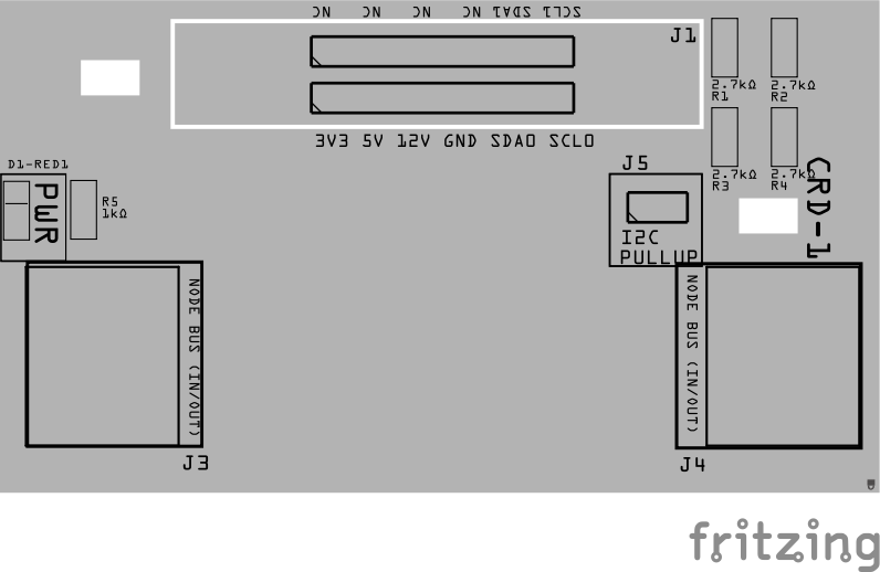
The illustration below shows the 2-slot LCC Fusion Node Bus Hub PCB variant. The top side of the PCB features one of the 805 card edge connectors (J1), positioned near the center-right of the board. Adjacent to this connector is the rectangular keyed card cutout notch, which ensures proper card orientation and prevents incorrect insertion.
Note that this image only shows the top side of the PCB; the second connector (J2) is mounted on the bottom side of the PCB, aligned with the top connector but not visible here.
This dual-sided connector configuration allows for compact bus expansion in limited space environments, such as under-layout installations.
![]()
Your paragraph text here will now wrap nicely on the left side of the image block. Add as much text as needed and it will flow around the floated block.
The following mechanical and electrical specifications apply to this and other Node Bus Hub variants, establishing the foundation for consistent card compatibility and system reliability.
| Variant | Approximate PCB Size | Number of Slots | Notes |
|---|---|---|---|
| Small (2-slot) | 100 mm × 50 mm | 2 | Fits under layout, compact |
| Medium (4-slot) | 170 mm × 50 mm | 4 | Standard desktop style |
| Large (6/8-slot) | 255–340 mm × 50 mm | 6 or 8 | Rack/centralized wiring |
Connectors
- Type: 805 Card Edge Connector (3.96mm pitch, 12 contacts)
- Orientation: Vertical insertion with keying to prevent mis insertion
- Spacing: 34.0 mm center-to-center between connectors (adjusted as needed)
- Mounting: PCB-mounted with plated through holes for mechanical strength
- Retention: Recommended use of retention clips or mechanical brackets for card stability
Mounting Holes
- Optional M3 mounting holes positioned along PCB edges
- Supports stacking, enclosure mounting, and strain relief
Keyed Card Rectangular Cutout (Mechanical Key)
To enforce correct card orientation and prevent damage, the Node Bus Hub PCB includes a rectangular cutout notch near the card edge connector, serving as a mechanical key.
| Parameter | Value (approximate) | Notes |
|---|---|---|
| Cutout shape | Rectangle | Must fit the mechanical key of the card |
| Width | 6.5 mm | Matches diameter of original circular keyhole |
| Height | 3.0 mm | Typical for keyed card notch height |
| Distance from connector pins | 10.2 mm (center of notch) | Measured from pin 1 centerline along PCB edge |
| Minimal Distance from PCB edge | 5.0 mm (center of notch) | Distance from PCB edge to center of notch |
| Position | Along PCB edge near connector | Same location as circular hole in previous design |
All hubs must include this notch for compatibility with keyed cards and consistent mechanical alignment.
Electrical Specifications
Node Bus Connectors
The Node Bus Hub RJ45 does not carry CAN. CAN is provided via a separate 2-wire connection to a Node Card or Power-CAN Card installed in the hub.
| Card Edge Socket | 8-pin header / RJ45 Socket | Name | Type | Description |
|---|---|---|---|---|
| 1 | 1 | 3.3 VDC | Power | 3.3 Volt power rail |
| 2 | 2 | 5 VDC | Power | 5 Volt power rail |
| 3 | 3 | 12 VDC | Power | 12 Volt power rail |
| 4 | 4 | GND | Power | Ground reference |
| 5 | 5 | I2C SDA0 | Signal | I2C bus 0 data line |
| 6 | 6 | I2C SCL0 | Signal | I2C bus 0 clock line |
| 7 | 7 | I2C SDA1 | Signal | I2C bus 1 data line |
| 8 | 8 | I2C SCL1 | Signal | I2C bus 1 clock line |
| 9 | N/A (via Node Card / Power-CAN Card) | CAN_H | Signal | CAN bus high differential line |
| 10 | N/A (via Node Card / Power-CAN Card) | CAN_L | Signal | CAN bus low differential line |
| 11 | N/A | DCC1 (Main Track) | Signal | Digital Command Control signal for the main running track. Supplies track power and control commands to locomotives operating on the main layout. This signal carries the standard DCC modulated waveform used for normal train operation. |
| 12 | N/A | DCC2 (Programming Track) | Signal | Digital Command Control signal for the programming track. Dedicated for programming and configuring decoders on locomotives, isolated from the main track signal to prevent interference with normal operation. Typically connected to a separate programming track section or booster. |
Power Distribution and Protection
- Power Rails: 3.3 VDC, 5 VDC, and 12 VDC rails supplied and distributed to all slots.
- Current Limits:
- 3.3 VDC rail rated for up to 1.5 A
- 5 VDC rail rated for up to 3 A
- 12 VDC rail rated for up to 1.5 A
- Protection Components:
- Reverse polarity protection diodes on all power inputs
- Resettable polyfuses for overcurrent protection
- Transient Voltage Suppression (TVS) diodes for spike protection
- Filtering: Bulk and decoupling capacitors on each rail reduce noise and ensure stable power delivery.
For implementation examples see the 6x Node Bus Hub Assembly Guide.
Communication Bus Specifications
- CAN Bus:
- Differential signaling on CAN_H and CAN_L lines (pins 5 & 6)
- 120 Ω termination resistors applied at bus endpoints or auto-termination circuits integrated into hubs
- Shielding and filtering components included to ensure signal integrity
- I2C Buses:
- Two independent I2C buses (SDA0/SCL0 and SDA1/SCL1) provided on pins 7-10
- Pull-up resistors and noise suppression ferrite beads recommended on hub and cards
- DCC Signals:
- High-voltage (~14–18 VDC peak-to-peak) modulated square waves on pins 11 and 12
- Electrical isolation and protection required on all interfacing cards to avoid damage
- Facilitates hybrid layouts running both LCC and traditional DCC control
For implementation examples see the 6x Node Bus Hub Assembly Guide.
Optional Features
- CAN Bus Auto-Termination: Circuitry to detect bus endpoints and automatically apply 120 Ω termination.
- Status and Diagnostic LEDs: Power and communication indicators for quick visual confirmation.
- Expansion Headers: Additional connectors for debugging, testing, or future feature expansion
References
- 6x Node Bus Hub Assembly Guide: Detailed build instructions, circuit diagrams, and optional component information.
- Node Card Assembly Guide: Reference for card-to-hub interfacing and card details.